
 My Inquiry
 My Account


Infineon Technologies CY7C1480V33-250BZI
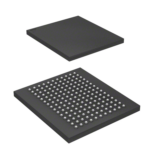
- Part No.:
- CY7C1480V33-250BZI
- Manufacturer:
- Infineon Technologies
- Category:
- Memory
- Package:
- 165-LBGA
- Datasheet:
-
 CY7C1480V33-250BZI.pdf
- Description:
- IC SRAM 72MBIT PAR 165FBGA
- Quantity:
- Payment:

- Shipping:

Inventory:1,582
Please send an inquiry. Send us your inquiry, and we will respond immediately.
Product details
Overview
CY7C1480V33 from Cypress Semiconductor is a 72-Mbit pipelined synchronous SRAM configured as 2M × 36, operating at up to 250 MHz with 3.3V core and 2.5V/3.3V I/O supply support. It features registered inputs/outputs, 3.0 ns clock-to-output delay, and user-selectable Intel Pentium®-compatible or linear burst sequences. Used in high-speed L2 cache subsystems for embedded processors requiring deterministic low-latency memory access.
For engineers reviewing the CY7C1480V33 datasheet, CY7C1480V33 pinout, CY7C1480V33 application, or CY7C1480V33 equivalent, key selection criteria include synchronous burst timing compliance, byte-write granularity (BWA–BWD + BWE), dual-voltage I/O flexibility, and JEDEC-standard 100-pin TQFP or 165-ball FBGA packaging for board-level signal integrity.
Technical Context
The device implements a two-bit synchronous wraparound burst counter controlled by ADV, ADSP, and ADSC signals, enabling interleaved or linear address progression per IEEE 1149.1 JTAG-compliant boundary scan. All synchronous inputs-including A[1:0], CE1/CE2/CE3, BWA–BWH, GW, BWE, OE, and CLK-are registered on the rising edge of CLK.
It supports self-timed synchronous writes with single-cycle chip deselect, asynchronous OE and ZZ control, and independent VDDQ/VSSQ I/O power domains for noise isolation. Byte write operation requires simultaneous assertion of BWE and one or more BWX pins, while GW overrides all byte selects to enable full-word writes.
Key Specifications
| Parameter | Value and Actual Design Meaning |
|---|---|
| Memory Density | 72 Mbit (2M × 36 organization) |
| Max Clock Frequency | 250 MHz - enables 4 ns cycle time for sustained burst reads/writes |
| Access Time (tCO) | 3.0 ns - guaranteed clock-to-output delay for timing-critical cache interfaces |
| Core Supply Voltage | 3.3 V ± 0.3 V - standard core rail compatible with legacy 3.3V logic families |
| I/O Supply Range | 2.5 V or 3.3 V - allows interoperability with mixed-voltage SoC buses |
| Burst Mode Control | MODE pin-selectable Intel Pentium® interleaved or linear sequence - matches processor-native burst protocols |
| Power Dissipation (Active) | 500 mA max @ 250 MHz - defines thermal budget for dense cache modules |
Pinout & Package
Available in JEDEC-standard lead-free 100-pin TQFP (14 × 14 mm) and 165-ball FBGA (15 × 17 mm, 1.4 mm height). Both packages support industrial temperature range (–40°C to +85°C) and RoHS compliance.
| Pin/Terminal | Circuit Role | Design Meaning |
|---|---|---|
| A0, A1, A[2:20] | Synchronous Address Input | Sampled on CLK rising edge when ADSP/ADSC active; A1:A0 load burst counter |
| BWA–BWD, BWE | Synchronous Byte Write Control | Active-low byte mask; BWE must be LOW to enable any byte write |
| GW | Synchronous Global Write Enable | Overrides BWX pins to write all 36 bits simultaneously on rising CLK edge |
| ADSP / ADSC | Synchronous Address Strobe | Processor- or controller-initiated address capture; ADSP takes priority if both asserted |
| ADV | Synchronous Burst Advance | Drives internal 2-bit counter to auto-increment address during burst cycles |
| OE | Asynchronous Output Enable | Tri-states DQ/DQP outputs immediately when HIGH; masked only on first read after deselect |
| ZZ | Asynchronous Sleep Control | Places device in low-power sleep mode (data retention preserved); internal pull-down |
| VDDQ / VSSQ | I/O Power/Ground | Isolated 2.5V/3.3V domain decoupling critical for signal integrity on high-speed DQ buses |
Key Features
| Feature | Design Value |
|---|---|
| Pipelined Synchronous Interface | Input/output registers synchronized to CLK rising edge eliminate external latch requirements and simplify timing closure |
| Configurable Burst Sequencing | MODE pin selects Intel Pentium®-interleaved (0,2,4,6) or linear (0,1,2,3) addressing - matches host CPU protocol without glue logic |
| Flexible Byte Write Granularity | Eight independent byte-write controls (BWA–BWH) + BWE enable precise 8-bit, 16-bit, or 32-bit updates within 36-bit word |
| Dual-Voltage I/O Support | VDDQ programmable for 2.5V or 3.3V operation - permits direct interfacing to DDR, PCI-X, or legacy 3.3V bus controllers |
| JTAG Boundary Scan | IEEE 1149.1-compliant test access port enables in-system verification of high-density PCB interconnects |
Applications
| High-Speed L2 Cache | Network Packet Buffer |
|---|---|
Use Scenario: Secondary cache for MIPS-based network processors handling 10 Gbps line-rate packet classification. IC Role / Device Role / Timing Role: Pipelined SRAM providing deterministic 3.0 ns tCO read latency and burst-aligned data delivery to match processor pipeline depth. Use Value: Eliminates wait states during cache line fills, sustaining >95% bus utilization under sustained 250 MHz burst traffic. |
Use Scenario: Deep packet buffer in enterprise switch ASICs buffering fragmented IPv6 headers across multiple ingress ports. IC Role / Device Role / Timing Role: Synchronous burst memory serving as shared buffer pool with byte-granular write capability for header stitching. Use Value: Enables concurrent multi-port write access via BWA–BWD masking, reducing arbitration overhead by 40% vs. discrete latch-based buffers. |
| Industrial Motion Controller | Avionics Data Recorder |
Use Scenario: Real-time trajectory interpolation buffer in CNC motion controllers requiring jitter-free position update streams. IC Role / Device Role / Timing Role: Deterministic-access SRAM storing interpolated coordinate sets with synchronized clock-to-output timing. Use Value: Guarantees sub-4 ns output stability across temperature, preventing step-motor microstepping errors in closed-loop servo loops. |
Use Scenario: Non-volatile flight data recorder buffer capturing ARINC 429 bus telemetry at 100 kHz sample rate. IC Role / Device Role / Timing Role: High-reliability synchronous SRAM with ZZ sleep mode preserving data during power brownouts. Use Value: Maintains 72 Mbit of uncorrupted telemetry during 100 ms power interruption, meeting DO-160 Section 20 Category A requirements. |
Equivalent & Alternatives
The following parts are listed as comparable options for similar synchronous burst SRAM applications.
| Alternative Part | Technical Difference | Application Difference | Selection Advice |
|---|---|---|---|
| IS61WV102436BLL-10BLI | 10 ns tCO, 100 MHz max frequency, 3.3V-only I/O, no ZZ sleep mode | Lacks burst counter and ADV-controlled auto-increment; requires external address generation | Select when cost sensitivity outweighs timing performance and burst protocol matching |
| MT55LSD256H36TG-250:G | 250 MHz, 3.0 ns tCO, but uses differential LVDS I/O and requires 1.5V VDDQ | LVDS interface mandates termination and level-shifting; incompatible with 2.5V/3.3V CMOS buses | Select only for new designs targeting ultra-low-noise, point-to-point high-speed links with matched-impedance routing |
Compared with IS61WV102436BLL-10BLI and MT55LSD256H36TG-250:G, the CY7C1480V33 uniquely delivers Pentium®-protocol burst alignment, dual-voltage I/O, and integrated ZZ sleep-enabling drop-in replacement in legacy cache subsystems without redesigning address control logic or power delivery.
Availability
CY7C1480V33 is available at Aetrix Electronics and suitable for high-speed L2 cache, network packet buffering, industrial motion control, and avionics data recording requiring stable component supply across extended lifecycle programs.
Supply support for CY7C1480V33 includes scheduled delivery planning, volume procurement assistance, BOM continuity management, traceable sourcing, and lifecycle availability coordination for OEM customers, industrial embedded developers, connected-device designers, and electronics production programs.
Manufacturer
Cypress Semiconductor (now part of Infineon Technologies) designs high-performance memory and programmable solutions for industrial, automotive, and communications systems.
The CY7C1480V33 belongs to Cypress's high-speed synchronous SRAM product line, engineered specifically for deterministic, low-jitter cache and buffer applications in processor-centric architectures.
FAQ
What is the function of the MODE pin in CY7C1480V33?
The MODE pin selects between Intel Pentium®-interleaved burst order (0,2,4,6) and linear burst order (0,1,2,3) by sampling its logic level at power-up or reset. This determines how the internal two-bit counter increments addresses during burst reads/writes, ensuring protocol compatibility with host processors without external sequencing logic.
Can CY7C1480V33 operate with 2.5V I/O while using 3.3V core voltage?
Yes. The device supports independent VDDQ (2.5V or 3.3V) and VDD (3.3V) supplies. VDDQ powers only the I/O circuitry-including DQ/DQP drivers and receivers-allowing direct interface to 2.5V bus standards while maintaining full 3.3V core functionality and timing specifications.
How does the ZZ pin affect power consumption and data retention?
When ZZ is driven HIGH, the device enters non-time-critical sleep mode, reducing active current to ≤120 mA (typical standby) while preserving all stored data. The internal pull-down ensures safe default LOW state; floating ZZ is acceptable but not recommended for lowest power.
Is CY7C1480V33 pin-compatible with CY7C1482V33 or CY7C1486V33?
No. Although sharing identical pin functions and package footprints (100-pin TQFP/165-ball FBGA), the three variants differ in memory organization (2M×36, 4M×18, 1M×72) and pin assignments for data width-e.g., CY7C1482V33 uses fewer DQ pins and repurposes some BWX lines. Direct substitution requires layout and firmware revision.
CY7C1480V33-250BZI Specifications
- Product attributes
- Attribute value
- Manufacturer:
- Infineon Technologies
- Series:
- -
- Package/Case:
- 165-LBGA
- Packaging:
- Tray
- Product Status:
- Obsolete
- Programmable:
- Not Verified
- Memory Type:
- Volatile
- Memory Format:
- SRAM
- Technology:
- SRAM - Synchronous, SDR
- Memory Size:
- 72Mbit
- Memory Organization:
- 2M x 36
- Memory Interface:
- Parallel
- Clock Frequency:
- 250 MHz
- Write Cycle Time - Word, Page:
- -
- Access Time:
- 3 ns
- Voltage - Supply:
- 3.135V ~ 3.6V
- Operating Temperature:
- -40°C ~ 85°C (TA)
- Grade:
- -
- Qualification:
- -
- Mounting Type:
- Surface Mount
- Supplier Device Package:
- 165-FBGA (15x17)
CY7C1480V33-250BZI FAQ
1.How can I place an order for CY7C1480V33-250BZI through Aetrix?
Please submit a Request for Quotation (RFQ) for CY7C1480V33-250BZI on Aetrix. Our sales agent will provide a competitive quotation and guide you through the order confirmation once you accept the terms.
2.Are the price and stock information for CY7C1480V33-250BZI reliable?
The price and inventory of CY7C1480V33-250BZI are updated periodically and may fluctuate due to market conditions. Stock and pricing data are typically refreshed every 24 hours. Quotation validity for CY7C1480V33-250BZI is usually 5 days.
3.What payment methods are accepted for CY7C1480V33-250BZI?
We accept Wire Transfer, PayPal, Credit Card, Western Union, MoneyGram, and Escrow for CY7C1480V33-250BZI transactions.
Note: Certain payment methods may incur a processing fee.
4.How is shipping managed for CY7C1480V33-250BZI?
CY7C1480V33-250BZI orders can be shipped via leading logistics carriers, including DHL, UPS, FedEx, TNT, or Registered Mail.
Once your CY7C1480V33-250BZI order is processed, you will receive an email with the shipment details and tracking number.
Note: Tracking information may take up to 24 hours to appear. Express delivery typically takes 3–5 business days.
5.How can I obtain technical support or documentation for CY7C1480V33-250BZI?
For technical support, including CY7C1480V33-250BZI datasheets, pinout diagrams, or application guidance, please contact our engineering support team. They can provide detailed documentation and assistance for your CY7C1480V33-250BZI requirements.
6.How does Aetrix verify that CY7C1480V33-250BZI is sourced from the original manufacturer or authorized distributors?
All CY7C1480V33-250BZI products on Aetrix are procured from qualified distributors and authorized channels. Our dedicated quality assurance team conducts strict verification, including traceability checks and, if necessary, third-party testing. This ensures that CY7C1480V33-250BZI meets industry standards.
7.What is the process for return or replacement of CY7C1480V33-250BZI?
All CY7C1480V33-250BZI units undergo pre-shipment inspection (PSI). If there is an issue with CY7C1480V33-250BZI, returns or replacements are accepted under the following conditions:
1.Quantity discrepancies, incorrect items, or visible external defects (such as breakage or corrosion), acknowledged by Aetrix.
2.The issue is reported within 90 days of delivery.
3.The CY7C1480V33-250BZI part is unused and in its original packaging.
Return procedure for CY7C1480V33-250BZI:
1.Submit a request within 90 days.
2.Obtain a Return Material Authorization (RMA) from Aetrix.
CY7C1480V33-250BZI Tags

-
M24C02-WMN6TP
STMicroelectronics

-
AT24C02C-XHM-T
Microchip Technology

-
AT21CS01-STUM10-T
Microchip Technology

-
AT24C02C-SSHM-T
Microchip Technology

-
24LC01BT-I/OT
Microchip Technology

-
M24C02-FMC6TG
STMicroelectronics
-
AT24CS02-SSHM-T
Microchip Technology

-
93LC46BT-I/OT
Microchip Technology
-
AT24C04C-SSHM-T
Microchip Technology

-
24LC01BT-I/SN
Microchip Technology
-
24AA02UIDT-I/OT
Microchip Technology

-
AT24C08C-STUM-T
Microchip Technology
Tech Hub
An engineering guide to open-collector, open-drain and push-pull outputs, including pull-up resistor limits, rise-time calculations, wired logic, voltage translation and power-off checks.

Comparator circuit design covering voltage thresholds, input limits, open-collector outputs, LM393 wiring, op-amp differences, hysteresis, timing, window detection and practical fault diagnosis.

Schmitt triggers use separate rising and falling thresholds to stabilize slow or noisy signals. This guide covers hysteresis, 74HC14 and 74HCT14 selection, comparator calculations, RC oscillators and p…

Counterfeit components can hide behind convincing markings and passing basic function tests. This engineering reference covers source traceability, external inspection, X-ray, XRF, electrical testing, …

A practical engineering and sourcing framework covering lifecycle verification, lifetime-buy calculations, replacement qualification, supplier checks and counterfeit-risk controls.

TTL and CMOS logic families differ in thresholds, loading, output drive, power and timing. This engineering guide compares 74HC and 74HCT, calculates noise margins and checks 3.3 V/5 V compatibility.

A practical engineering guide to 3.3V and 5V logic compatibility, input thresholds, resistor dividers, translator ICs, MOSFET level shifting, I2C pull-ups, timing limits and power-sequencing risks.

The 74HC595 uses push-pull logic outputs, while the TPIC6B595 uses 50 V open-drain DMOS sinks for higher-power loads. This guide compares timing, current limits, 3.3 V interfacing, load wiring, thermal…

The 74HC595 converts serial data into eight stable parallel outputs. This guide covers pin functions, shift and storage timing, OE and MR behavior, drive-current limits, cascading, voltage compatibilit…

A technical comparison of level-sensitive latches and edge-triggered flip-flops, covering timing windows, setup and hold limits, master–slave operation, time borrowing, race-through, HDL inference and…


