
 My Inquiry
 My Account


Infineon Technologies CY7C53150-20AXI
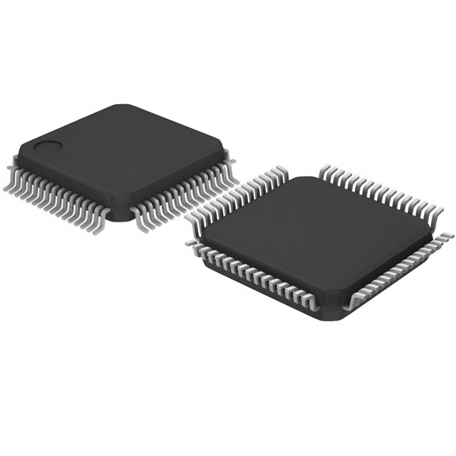
- Part No.:
- CY7C53150-20AXI
- Manufacturer:
- Infineon Technologies
- Category:
- Application Specific Microcontrollers
- Package:
- 64-LQFP
- Datasheet:
-
 CY7C53150-20AXI.pdf
- Description:
- IC PROCESSOR NEURON 64LQFP
- Quantity:
- Payment:

- Shipping:

Inventory:2,480
Please send an inquiry. Send us your inquiry, and we will respond immediately.
Product details
Overview
CY7C53150-20AXI from Cypress Semiconductor is a Neuron Chip network processor implementing a full LonWorks node on a single die, integrating three 8-bit pipelined processors (application, network, MAC), 2 KB SRAM, 512 bytes of on-chip Flash, external memory interface addressing up to 58 KB, and a 5-pin programmable communications port supporting twisted-pair, powerline, and RF transceivers in industrial building automation systems.
For engineers reviewing the CY7C53150-20AXI datasheet, CY7C53150-20AXI pinout, CY7C53150-20AXI application, or CY7C53150-20AXI equivalent, key selection criteria include its 20 MHz max clock operation, 64-pin TQFP package with 11-pin I/O port configurable in 34 modes, 20 mA sink capability on I/O0–I/O3, unique 48-bit ID, and LVD circuit for nonvolatile memory protection during voltage drops.
Technical Context
The device implements all seven OSI layers via 10 KB of embedded LonTalk protocol firmware stored in ROM - unlike CY7C53120 variants, CY7C53150 requires system firmware to reside in off-chip nonvolatile memory (e.g., Flash/EPROM) within the first 16 KB address space. Its external memory interface supports 16-bit address bus (A0–A15), 8-bit data bus (D0–D7), and control signals E and R/W.
Three independent 8-bit processors execute concurrently: the Application Processor runs user code stored in on-chip Flash and/or external memory; the Network Processor handles packet assembly/disassembly; and the Media Access Control Processor manages physical-layer timing and collision detection. The communications port operates in Single-Ended, Special Purpose, or Differential Mode using Differential Manchester encoding.
Key Specifications
| Parameter | Value and Actual Design Meaning |
|---|---|
| Max Clock Frequency | 20 MHz - determines maximum instruction throughput and network data rate compatibility with LonWorks 78 kbps standard. |
| SRAM Size | 2,048 bytes - buffers inbound/outbound network packets and stores runtime variables for concurrent application and protocol stacks. |
| On-Chip Flash | 512 bytes - stores boot configuration, node-specific parameters, and small application segments; supports 100,000 erase/write cycles with 10-year data retention. |
| External Memory Address Space | Up to 58 KB - enables large application programs and firmware updates without requiring chip replacement. |
| I/O Sink Current | 20 mA on I/O0–I/O3 - directly drives LEDs, relays, or logic inputs without external drivers in sensor/actuator interfaces. |
| LVD Threshold | 4.1 V ± 0.3 V - prevents flash corruption during brown-out conditions by halting writes when VDD falls below safe operating level. |
| Operating Voltage | 5.0 V nominal - compatible with legacy industrial 5 V supply rails and simplifies power design versus mixed-voltage SoCs. |
Pinout & Package
Package: 64-pin Thin Quad Flat Package (TQFP), 10 mm × 10 mm, 0.5 mm pitch, RoHS-compliant, thermal resistance θJA = 44 °C/W.
| Pin/Terminal | Circuit Role | Design Meaning |
|---|---|---|
| CLK1 | Oscillator input / external clock source | Accepts crystal (with CLK2) or TTL-level 20 MHz clock; must be stable before release from RESET. |
| I/O0–I/O3 | General-purpose I/O with high-sink drive | 20 mA sink capability enables direct connection to indicators or low-side switches; Timer1/2 outputs routable to I/O0/I/O1. |
| I/O4–I/O7 | General-purpose I/O with programmable pull-ups | Support timer input capture; pull-up configuration reduces external component count in switch/sensor interfaces. |
| CP0–CP4 | Differential communications port | Configurable for Single-Ended, Special Purpose, or Differential Mode; CP0/CP1 form receiver pair, CP2/CP3 driver pair in differential mode. |
| A0–A15, D0–D7, E, R/W | External memory interface bus | Enables expansion beyond on-chip resources; A15 maps to 64 KB boundary but only 58 KB usable due to internal register mapping. |
| SERVICE | Active-low service pin | Self-toggles at 76 Hz for diagnostic polling; used during installation to identify nodes on powered networks. |
| RESET | Active-low reset with built-in pull-up | Requires 100–1000 pF external capacitance for proper debouncing; initiates cold start and firmware reload sequence. |
Key Features
| Feature | Design Value |
|---|---|
| Triple 8-bit pipelined processors | Enables true concurrency: application logic, LonTalk protocol stack, and media access control execute independently without software scheduling overhead. |
| 11-pin I/O port with 34 programmable modes | Reduces firmware development time for custom sensor/actuator interfaces by eliminating bit-banging and enabling hardware-assisted waveform generation. |
| Two 16-bit timer/counters | Support precise pulse-width measurement (e.g., HVAC valve position feedback) and generation (e.g., PWM fan control) with input capture from I/O4–I/O7. |
| Unique 48-bit ID per device | Eliminates manual node addressing during commissioning; enables automated topology discovery and firmware deployment across large-scale building networks. |
| On-chip LVD circuit | Guarantees flash write integrity during transient line sags - critical for field-updatable nodes deployed in electrically noisy industrial environments. |
Applications
| Building Automation System Node | Industrial HVAC Controller |
|---|---|
Use Scenario: Distributed temperature, humidity, and occupancy sensing across multi-floor commercial buildings using twisted-pair wiring. IC Role / Device Role / Timing Role: Full LonWorks node executing application logic, LonTalk protocol stack, and MAC layer timing - no external microcontroller or protocol accelerator required. Use Value: Reduces BOM count by integrating all networking intelligence into one IC; 48-bit ID enables zero-touch commissioning of 100+ nodes per network segment. | Use Scenario: Local control of chillers, air handlers, and VAV boxes with analog sensor inputs and relay/valve actuator outputs. IC Role / Device Role / Timing Role: Real-time I/O processing unit with 20 mA sink on I/O0–I/O3 driving relays directly; timers measure thermistor RC decay for precision temperature calculation. Use Value: Eliminates external driver ICs and discrete timing components; 11-pin I/O port configured in PWM mode controls damper actuators with <1% duty cycle resolution. |
| Smart Lighting Node | Powerline Communication Gateway |
Use Scenario: DALI-to-LonWorks bridge controlling LED luminaires over AC powerlines in retrofit office installations. IC Role / Device Role / Timing Role: Communications port configured in Special Purpose Mode to interface with intelligent DALI transceiver; SERVICE pin used for manual lamp group identification. Use Value: Enables legacy DALI infrastructure to join LonWorks management network without protocol translation gateways or host processors. | Use Scenario: Residential energy monitoring hub communicating with smart meters and appliance controllers via powerline medium. IC Role / Device Role / Timing Role: Communications port in Differential Mode with programmable hysteresis (H=3) and glitch filter (F=2) optimized for noisy 120 VAC environments. Use Value: Achieves >99.9% packet success rate at 56 kbps over 300 m of residential wiring; on-chip LVD prevents firmware corruption during brownouts common in grid-edge devices. |
Equivalent & Alternatives
The following parts are listed as comparable options for similar LonWorks node applications.
| Alternative Part | Technical Difference | Application Difference | Selection Advice |
|---|---|---|---|
| MC143150Bx | Pin-compatible Motorola predecessor; identical 64-pin TQFP footprint and memory map but lacks on-chip Flash and uses older 0.8 µm process. | No in-field firmware update capability; requires EPROM programmer for every code change. | Select MC143150Bx only for legacy board rework where Flash programmability is unnecessary. |
| TMPN3150B1 | Toshiba equivalent with same pinout and electrical specs; ROM-based firmware only - no on-chip Flash or external memory interface. | Fixed-function node; cannot host user application code beyond factory-loaded firmware. | Choose TMPN3150B1 for cost-sensitive, static-function deployments where field upgrades are not required. |
Compared with MC143150Bx and TMPN3150B1, CY7C53150-20AXI provides field-upgradable application code via on-chip Flash and external memory expansion, enabling adaptive control logic and remote diagnostics - essential for modern building management systems requiring long-term software maintainability.
Availability
CY7C53150-20AXI is available at Aetrix Electronics and suitable for building automation systems, industrial HVAC controllers, smart lighting nodes, and powerline communication gateways requiring stable component supply across extended product lifecycles.
Supply support for CY7C53150-20AXI includes scheduled delivery planning, volume procurement assistance, BOM continuity management, traceable sourcing, and lifecycle availability coordination for OEM customers, industrial embedded developers, connected-device designers, and electronics production programs.
Manufacturer
Cypress Semiconductor (now part of Infineon Technologies) is a U.S.-based semiconductor company specializing in microcontrollers, connectivity solutions, and programmable system-on-chip devices for industrial, automotive, and IoT applications.
CY7C53150 belongs to the Neuron Chip product line, designed specifically to implement standards-compliant LonWorks nodes with integrated protocol stack, deterministic real-time I/O, and robust noise-immune communications for distributed building and industrial control networks.
FAQ
What is the role of the SERVICE pin in CY7C53150-20AXI?
The SERVICE pin is an active-low, self-toggling I/O that alternates between input and output at 76 Hz. During network installation, it enables physical identification of powered nodes by causing connected LEDs to blink or triggering audible indicators. It also serves as a hardware handshake signal during firmware download sequences and supports diagnostic polling without requiring network traffic.
Can CY7C53150-20AXI operate without external memory?
Yes - CY7C53150-20AXI can execute basic functions using its 2 KB SRAM and 512-byte on-chip Flash for configuration storage. However, full LonTalk system firmware must reside in the first 16 KB of external nonvolatile memory (e.g., Flash/EPROM); the chip will not initialize without it. External memory is mandatory for operational deployment, though minimal test modes may run with RAM-only initialization.
How does the communications port support different transceiver types?
The 5-pin CP0–CP4 port supports three configurations: Single-Ended Mode (CP0 receive, CP1 transmit, CP2 enable) for basic RS-485 transceivers; Special Purpose Mode (CP0/CP1 data, CP2 bit clock, CP4 frame clock) for intelligent transceivers like DALI bridges; and Differential Mode (CP0/CP1 receiver, CP2/CP3 driver) for noise-immune twisted-pair or powerline interfaces with programmable hysteresis and glitch filtering.
What is the purpose of the LVD circuit in CY7C53150-20AXI?
The on-chip Low-Voltage Inhibit (LVD) circuit monitors VDD and disables flash write operations when voltage drops below 4.1 V ± 0.3 V. This prevents bit corruption during brown-out events - a critical reliability feature for field-deployed nodes subject to unstable mains power or battery sag, ensuring firmware and configuration integrity remains intact across thousands of power cycles.
CY7C53150-20AXI Specifications
- Product attributes
- Attribute value
- Manufacturer:
- Infineon Technologies
- Series:
- Neuron®
- Package/Case:
- 64-LQFP
- Packaging:
- Tray
- Product Status:
- Obsolete
- Programmable:
- Not Verified
- Applications:
- Network Processor
- Core Processor:
- Pipelined
- Program Memory Type:
- FLASH (512 B)
- Controller Series:
- CY7C531xx
- RAM Size:
- 2K x 8
- Interface:
- Serial
- Number of I/O:
- 19
- Voltage - Supply:
- 4.5V ~ 5.5V
- Operating Temperature:
- -40°C ~ 85°C
- Grade:
- -
- Qualification:
- -
- Mounting Type:
- Surface Mount
- Supplier Device Package:
- 64-TQFP (14x14)
CY7C53150-20AXI FAQ
1.How can I place an order for CY7C53150-20AXI through Aetrix?
Please submit a Request for Quotation (RFQ) for CY7C53150-20AXI on Aetrix. Our sales agent will provide a competitive quotation and guide you through the order confirmation once you accept the terms.
2.Are the price and stock information for CY7C53150-20AXI reliable?
The price and inventory of CY7C53150-20AXI are updated periodically and may fluctuate due to market conditions. Stock and pricing data are typically refreshed every 24 hours. Quotation validity for CY7C53150-20AXI is usually 5 days.
3.What payment methods are accepted for CY7C53150-20AXI?
We accept Wire Transfer, PayPal, Credit Card, Western Union, MoneyGram, and Escrow for CY7C53150-20AXI transactions.
Note: Certain payment methods may incur a processing fee.
4.How is shipping managed for CY7C53150-20AXI?
CY7C53150-20AXI orders can be shipped via leading logistics carriers, including DHL, UPS, FedEx, TNT, or Registered Mail.
Once your CY7C53150-20AXI order is processed, you will receive an email with the shipment details and tracking number.
Note: Tracking information may take up to 24 hours to appear. Express delivery typically takes 3–5 business days.
5.How can I obtain technical support or documentation for CY7C53150-20AXI?
For technical support, including CY7C53150-20AXI datasheets, pinout diagrams, or application guidance, please contact our engineering support team. They can provide detailed documentation and assistance for your CY7C53150-20AXI requirements.
6.How does Aetrix verify that CY7C53150-20AXI is sourced from the original manufacturer or authorized distributors?
All CY7C53150-20AXI products on Aetrix are procured from qualified distributors and authorized channels. Our dedicated quality assurance team conducts strict verification, including traceability checks and, if necessary, third-party testing. This ensures that CY7C53150-20AXI meets industry standards.
7.What is the process for return or replacement of CY7C53150-20AXI?
All CY7C53150-20AXI units undergo pre-shipment inspection (PSI). If there is an issue with CY7C53150-20AXI, returns or replacements are accepted under the following conditions:
1.Quantity discrepancies, incorrect items, or visible external defects (such as breakage or corrosion), acknowledged by Aetrix.
2.The issue is reported within 90 days of delivery.
3.The CY7C53150-20AXI part is unused and in its original packaging.
Return procedure for CY7C53150-20AXI:
1.Submit a request within 90 days.
2.Obtain a Return Material Authorization (RMA) from Aetrix.
CY7C53150-20AXI Tags

-
CYPD3175-24LQXQ
Infineon Technologies

-
SLB9672VU20FW1523XTMA1
Infineon Technologies

-
SLB9670VQ20FW785XTMA1
Infineon Technologies
-
SLB9672XU20FW1523XTMA1
Infineon Technologies
-
SLB9673XU20FW2613XTMA1
Infineon Technologies

-
CYPD3125-40LQXIT
Infineon Technologies

-
AT97SC3204-U2A1A-20
Microchip Technology
-
AT97SC3204-U2A1A-10
Microchip Technology
-
SLM9670AQ20FW1311XTMA1
Infineon Technologies
-
SLB9672XU20FW1613XTMA1
Infineon Technologies
-
SLB9672AU20FW1613XTMA1
Infineon Technologies
-
SLB9673AU20FW2613XTMA1
Infineon Technologies
Tech Hub

18650 battery guide covering lithium-ion cell basics, 3.6V/3.7V voltage, 4.2V charging, mAh and Wh capacity, protected cells, chargers, BMS, series-parallel packs, holders, welding and sourcing checks.…

Hall effect sensor guide covering working principle, linear and digital sensors, Arduino circuits, current sensing, speed detection, automotive applications, A3144 examples, signal filtering and datash…

Product Change Notification guide for electronic components, covering PCN meaning, PCN vs PDN/EOL, common change types, risk levels, form-fit-function review, engineering validation, BOM control, LTB/L…

A practical guide to blend door actuators, covering HVAC function, symptoms, location, AC and heater issues, reset and calibration, replacement cost, electrical diagnosis, compatibility checks, and rep…

Engineering guide to Raspberry Pi alternatives, covering chip-level differences, Orange Pi, ROCK, Jetson, Banana Pi, NanoPi, Compute Module, Pico, GPIO, camera, HAT compatibility, and replacement risks…

Engineering guide to dynamic load response testing for high-current buck converters, covering load step setup, slew rate, Vcore undershoot, overshoot, recovery time, probe location, output capacitors a…

Engineering guide to output capacitor selection for ASIC Vcore rails, covering bulk capacitors, polymer capacitors, MLCC decoupling, DC bias, ESR, ESL, placement, transient response and substitution ri…

Engineering guide to high-current ASIC Vcore rails, covering 12-phase buck architecture, PMBus control, dynamic load testing, output capacitor networks, smart power stage selection, thermal design and …

Voltage regulator guide covering linear, LDO, 7805, Zener, adjustable, buck, VRM and alternator regulators, with design checks, testing methods, troubleshooting and datasheet-based selection.

Amplifier guide covering voltage, current and power amplification, gain, feedback, amplifier classes, audio and RF applications, op-amp circuits, transimpedance amplifiers, datasheet selection and trou…


