
 My Inquiry
 My Account


Infineon Technologies CY7C68000-56LFXC
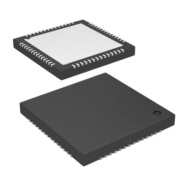
- Part No.:
- CY7C68000-56LFXC
- Manufacturer:
- Infineon Technologies
- Category:
- Drivers, Receivers, Transceivers
- Package:
- 56-VFQFN Exposed Pad
- Datasheet:
-
 CY7C68000-56LFXC.pdf
- Description:
- IC TRANSCEIVER FULL 1/1 56QFN
- Quantity:
- Payment:

- Shipping:

Inventory:4,620
Please send an inquiry. Send us your inquiry, and we will respond immediately.
Product details
Overview
CY7C68000-56LFXC from Cypress Semiconductor is a USB 2.0 UTMI-compliant transceiver IC that implements the physical layer (PHY) for high-speed (480 Mbps) and full-speed (12 Mbps) USB device operation. It provides serial-to-parallel conversion via an 8-bit/60-MHz or 16-bit/30-MHz parallel interface, integrates internal 1.5-kΩ DPLUS pull-up and USB line terminations, and operates from a single 3.3 V supply with an on-chip 24-MHz crystal oscillator interface - used in DSL modems and memory card readers.
For engineers reviewing the CY7C68000-56LFXC datasheet, CY7C68000-56LFXC pinout, CY7C68000-56LFXC application, or CY7C68000-56LFXC equivalent, key selection criteria include UTMI v1.05 compliance, integrated analog termination, dual-speed mode control (XcvrSelect/TermSelect), synchronous LineState[1:0] output, and OpMode-selectable test modes including bit-stuffing disable.
Technical Context
The CY7C68000 implements a dual-mode USB 2.0 PHY with independent FS and HS transceiver paths selected by XcvrSelect and termination control via TermSelect. Its on-die 24-MHz oscillator drives a PLL generating 30 MHz (16-bit mode) or 60 MHz (8-bit mode) UTMI clock, synchronized to CLK output.
It performs real-time NRZI encoding/decoding, bit stuffing/unstuffing with error detection, EOP/SYNC generation/detection, and elastic buffering to absorb data rate variation. LineState[1:0] outputs mirror DMINUS/DPLUS states synchronously to CLK, enabling precise bus state monitoring in host-side glue logic.
Key Specifications
| Parameter | Value and Actual Design Meaning |
|---|---|
| USB Speed Modes | High Speed (480 Mbps) and Full Speed (12 Mbps); no Low Speed support. |
| UTMI Compliance | UTMI+ v1.05 specification compliant; certified for USB 2.0 device operation. |
| Parallel Interface | Configurable 8-bit @ 60 MHz or 16-bit @ 30 MHz bidirectional data bus. |
| Supply Voltage | 3.3 V ±10%; AVCC and VCC rails separately decoupled for analog/digital isolation. |
| Crystal Input | 24 MHz ±100 ppm parallel-resonant fundamental-mode crystal; internal oscillator circuit. |
| Integrated Termination | On-chip 1.5-kΩ DPLUS pull-up and USB differential line terminations; no external resistors required. |
| Operational Modes | OpMode[1:0] selects Normal (00), Non-driving (01), or Bit-Stuff/NRZI Disable (10). |
Pinout & Package
Package: 56-pin QFN (7 mm × 7 mm, 0.5 mm pitch) - RoHS-compliant, thermally enhanced, lead-free.
| Pin/Terminal | Circuit Role | Design Meaning |
|---|---|---|
| D[15:0] | Bidirectional Data Bus | 16-bit parallel interface; D[7:0] active in 8-bit mode; ValidH controls upper byte validity in 16-bit mode. |
| CLK | Output Clock | Synchronous 30 MHz (16-bit) or 60 MHz (8-bit) clock for data capture; sourced from internal PLL. |
| XcvrSelect / TermSelect | Input Control Signals | XcvrSelect = 0 enables HS transceiver; TermSelect = 0 enables HS termination (SE0 assertion). |
| LineState[1:0] | Output Bus State Monitor | Synchronized combinatorial outputs reflecting DMINUS (LineState1) and DPLUS (LineState0) states per USB J/K/SE0 definitions. |
| XTALIN / XTALOUT | Clock Oscillator Interface | 24-MHz crystal connection points; supports external square-wave clock on XTALIN only. |
| Reset | Active-High Asynchronous Reset | Resets entire chip; internal PLL stabilizes ~200 µs after VCC reaches 3.3 V. |
Key Features
| Feature | Design Value |
|---|---|
| Integrated USB Analog Front-End | Eliminates external 1.5-kΩ pull-up and D+/D− termination resistors, reducing BOM count and PCB area. |
| UTMI+ v1.05 Interface | Standardized parallel interface enables seamless integration with USB controller ASICs or FPGA-based SIEs without custom PHY glue logic. |
| Dynamic Speed Mode Switching | XcvrSelect and TermSelect pins allow runtime switching between FS and HS operation, supporting USB enumeration and speed negotiation. |
| Synchronous Line State Monitoring | LineState[1:0] outputs aligned to CLK enable deterministic bus state sampling in digital logic, critical for protocol analyzers and debug tools. |
| Test Mode Flexibility | OpMode[1:0] supports non-driving (soft disconnect) and NRZI/buffer bypass modes for USB compliance testing and signal integrity validation. |
Applications
| DSL Modem Interface | Memory Card Reader |
|---|---|
|
Use Scenario: High-bandwidth bridging between USB host and ADSL chipset using parallel FIFO interface. IC Role / Device Role / Timing Role: USB 2.0 PHY providing HS/FS signaling, clock recovery, and NRZI encoding for upstream data transmission. Use Value: Enables 480 Mbps aggregate throughput while offloading analog USB timing and impedance matching from the modem SoC. |
Use Scenario: Compact SD/microSD reader connecting to PC via USB 2.0 with minimal external components. IC Role / Device Role / Timing Role: Physical layer transceiver handling USB packet serialization, SYNC/EOP framing, and line-state detection. Use Value: Reduces bill-of-materials by integrating all USB termination and biasing, supporting Class 10 UHS-I card read speeds over USB. |
| Legacy Device Converter | USB Camera Module |
|
Use Scenario: Converting parallel ATA or IDE signals to USB 2.0 for legacy storage device connectivity. IC Role / Device Role / Timing Role: UTMI interface bridge converting burst-mode ATA transfers into USB token/data packets with elastic buffering. Use Value: Eliminates need for discrete USB PHY + controller combo; supports both 8-bit unidirectional and 16-bit bidirectional host-side interfaces. |
Use Scenario: Embedded camera subsystem transmitting MJPEG video streams to host PC at sustained 24–30 fps. IC Role / Device Role / Timing Role: High-speed USB PHY managing 480 Mbps data flow, clock recovery, and bit-stuffing compensation for variable-bitrate video payloads. Use Value: Maintains frame synchronization via RXValid/TXReady handshaking and LineState monitoring during hot-plug and suspend/resume transitions. |
Equivalent & Alternatives
The following parts are listed as comparable options for similar USB 2.0 UTMI transceiver applications.
| Alternative Part | Technical Difference | Application Difference | Selection Advice |
|---|---|---|---|
| ISP1504A (NXP) | Single 3.3 V supply; no integrated crystal oscillator - requires external 48 MHz clock or crystal. | Lacks on-chip 24-MHz oscillator and PLL; demands external clock source or separate oscillator circuit. | Select when system already provides 48 MHz reference or when lower analog power consumption is prioritized over integration. |
| USB3300 (Microchip) | Supports UTMI+ v1.05 and ULPI; includes integrated USB charger detection (BC1.2) and VBUS sensing. | Enables charging port functionality and VBUS monitoring not present in CY7C68000; adds pin count and complexity. | Select when USB battery charging compliance or VBUS-aware power management is required alongside transceiver operation. |
Compared with ISP1504A and USB3300, the CY7C68000-56LFXC offers highest integration for cost-sensitive USB 2.0 device PHYs with built-in oscillator and zero-external-resistor termination, but lacks BC1.2 or ULPI support needed for newer host-facing or charging-aware designs.
Availability
CY7C68000-56LFXC is available at Aetrix Electronics and suitable for DSL modems, memory card readers, and legacy conversion devices requiring stable component supply, long-term lifecycle support, and RoHS-compliant QFN packaging.
Supply support for CY7C68000-56LFXC includes scheduled delivery planning, volume procurement assistance, BOM continuity management, traceable sourcing, and lifecycle availability coordination for OEM customers, industrial embedded developers, connected-device designers, and electronics production programs.
Manufacturer
Cypress Semiconductor (now part of Infineon Technologies) designs high-performance mixed-signal ICs for USB, memory, PSoC, and programmable logic applications.
The EZ-USB TX2™ product line delivers fully integrated USB 2.0 PHYs targeting cost-sensitive, space-constrained USB peripheral designs where analog front-end integration reduces design risk and time-to-market.
FAQ
Does CY7C68000-56LFXC support Low-Speed (1.5 Mbps) USB operation?
No. The CY7C68000-56LFXC supports only Full Speed (12 Mbps) and High Speed (480 Mbps) USB 2.0 signaling modes. It explicitly excludes Low-Speed operation per its functional specification and block diagram - no LS transceiver path or related control logic is implemented.
What is the role of the DataBus16_8 and Uni_Bidi pins?
DataBus16_8 configures the parallel interface width: logic HIGH enables 16-bit/30-MHz mode; LOW enables 8-bit/60-MHz mode. Uni_Bidi, active HIGH only in 8-bit mode, switches D[0:7] between bidirectional (Uni_Bidi = 0) and unidirectional Rx/Tx split (Uni_Bidi = 1), altering data bus timing behavior.
Can CY7C68000-56LFXC operate without an external crystal?
No. The device requires a 24-MHz parallel-resonant fundamental-mode crystal connected between XTALIN and XTALOUT. While XTALIN accepts an external 24-MHz square wave, no internal RC oscillator or clock multiplier replaces the crystal requirement - PLL operation depends on this reference.
How does the CY7C68000 handle USB suspend/resume signaling?
It detects USB suspend via the Suspend input pin and enters low-power mode, shutting down non-essential blocks. Resume signaling is generated by driving the D+/D− lines per USB 2.0 spec; TermSelect must remain in FS mode during suspend to maintain DPLUS pull-up, ensuring upstream port recognizes resume handshake.
CY7C68000-56LFXC Specifications
- Product attributes
- Attribute value
- Manufacturer:
- Infineon Technologies
- Series:
- CY7C
- Package/Case:
- 56-VFQFN Exposed Pad
- Packaging:
- Tube
- Product Status:
- Obsolete
- Type:
- Transceiver
- Protocol:
- USB 2.0
- Number of Drivers/Receivers:
- 1/1
- Duplex:
- Full
- Receiver Hysteresis:
- -
- Data Rate:
- -
- Voltage - Supply:
- 3V ~ 3.6V
- Operating Temperature:
- 0°C ~ 70°C
- Grade:
- -
- Qualification:
- -
- Mounting Type:
- Surface Mount
- Supplier Device Package:
- 56-QFN (8x8)
CY7C68000-56LFXC FAQ
1.How can I place an order for CY7C68000-56LFXC through Aetrix?
Please submit a Request for Quotation (RFQ) for CY7C68000-56LFXC on Aetrix. Our sales agent will provide a competitive quotation and guide you through the order confirmation once you accept the terms.
2.Are the price and stock information for CY7C68000-56LFXC reliable?
The price and inventory of CY7C68000-56LFXC are updated periodically and may fluctuate due to market conditions. Stock and pricing data are typically refreshed every 24 hours. Quotation validity for CY7C68000-56LFXC is usually 5 days.
3.What payment methods are accepted for CY7C68000-56LFXC?
We accept Wire Transfer, PayPal, Credit Card, Western Union, MoneyGram, and Escrow for CY7C68000-56LFXC transactions.
Note: Certain payment methods may incur a processing fee.
4.How is shipping managed for CY7C68000-56LFXC?
CY7C68000-56LFXC orders can be shipped via leading logistics carriers, including DHL, UPS, FedEx, TNT, or Registered Mail.
Once your CY7C68000-56LFXC order is processed, you will receive an email with the shipment details and tracking number.
Note: Tracking information may take up to 24 hours to appear. Express delivery typically takes 3–5 business days.
5.How can I obtain technical support or documentation for CY7C68000-56LFXC?
For technical support, including CY7C68000-56LFXC datasheets, pinout diagrams, or application guidance, please contact our engineering support team. They can provide detailed documentation and assistance for your CY7C68000-56LFXC requirements.
6.How does Aetrix verify that CY7C68000-56LFXC is sourced from the original manufacturer or authorized distributors?
All CY7C68000-56LFXC products on Aetrix are procured from qualified distributors and authorized channels. Our dedicated quality assurance team conducts strict verification, including traceability checks and, if necessary, third-party testing. This ensures that CY7C68000-56LFXC meets industry standards.
7.What is the process for return or replacement of CY7C68000-56LFXC?
All CY7C68000-56LFXC units undergo pre-shipment inspection (PSI). If there is an issue with CY7C68000-56LFXC, returns or replacements are accepted under the following conditions:
1.Quantity discrepancies, incorrect items, or visible external defects (such as breakage or corrosion), acknowledged by Aetrix.
2.The issue is reported within 90 days of delivery.
3.The CY7C68000-56LFXC part is unused and in its original packaging.
Return procedure for CY7C68000-56LFXC:
1.Submit a request within 90 days.
2.Obtain a Return Material Authorization (RMA) from Aetrix.
CY7C68000-56LFXC Tags

-
ATA6561-GAQW-N
Microchip Technology
-
ATA6561-GBQW-N
Microchip Technology

-
AM26LS32ACDR
Texas Instruments

-
SP485CN-L/TR
MaxLinear, Inc.
-
SP485EN-L/TR
MaxLinear, Inc.
-
SP485EEN-L/TR
MaxLinear, Inc.
-
SP485ECN-L/TR
MaxLinear, Inc.
-
THVD1400DR
Texas Instruments
-
AM26C31IDR
Texas Instruments

-
TLIN1021ADRQ1
Texas Instruments
-
MAX232IDR
Texas Instruments
-
AM26C32IDR
Texas Instruments
Tech Hub

Conditional Access Module guide covering CAM meaning, CI/CI+ interface, smart card authorization, DVB security workflow, TV and set-top box compatibility, internal electronics, ESD protection, connecto…

Guide to electronic component obsolescence covering EOL risk, PCN/PDN notices, last-time buy planning, replacement options, form-fit-function validation, counterfeit risk and BOM lifecycle management.

18650 battery guide covering lithium-ion cell basics, 3.6V/3.7V voltage, 4.2V charging, mAh and Wh capacity, protected cells, chargers, BMS, series-parallel packs, holders, welding and sourcing checks.…

Hall effect sensor guide covering working principle, linear and digital sensors, Arduino circuits, current sensing, speed detection, automotive applications, A3144 examples, signal filtering and datash…

Product Change Notification guide for electronic components, covering PCN meaning, PCN vs PDN/EOL, common change types, risk levels, form-fit-function review, engineering validation, BOM control, LTB/L…

A practical guide to blend door actuators, covering HVAC function, symptoms, location, AC and heater issues, reset and calibration, replacement cost, electrical diagnosis, compatibility checks, and rep…

Engineering guide to Raspberry Pi alternatives, covering chip-level differences, Orange Pi, ROCK, Jetson, Banana Pi, NanoPi, Compute Module, Pico, GPIO, camera, HAT compatibility, and replacement risks…

Engineering guide to dynamic load response testing for high-current buck converters, covering load step setup, slew rate, Vcore undershoot, overshoot, recovery time, probe location, output capacitors a…

Engineering guide to output capacitor selection for ASIC Vcore rails, covering bulk capacitors, polymer capacitors, MLCC decoupling, DC bias, ESR, ESL, placement, transient response and substitution ri…

Engineering guide to high-current ASIC Vcore rails, covering 12-phase buck architecture, PMBus control, dynamic load testing, output capacitor networks, smart power stage selection, thermal design and …


