
 My Inquiry
 My Account


Infineon Technologies CY7C68000-56PVXC
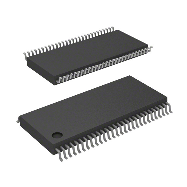
- Part No.:
- CY7C68000-56PVXC
- Manufacturer:
- Infineon Technologies
- Category:
- Drivers, Receivers, Transceivers
- Package:
- 56-BSSOP (0.295", 7.50mm Width)
- Datasheet:
-
 CY7C68000-56PVXC.pdf
- Description:
- IC TRANSCEIVER FULL 1/1 56SSOP
- Quantity:
- Payment:

- Shipping:

Inventory:1,860
Please send an inquiry. Send us your inquiry, and we will respond immediately.
Product details
Overview
CY7C68000-56PVXC from Cypress Semiconductor is a USB 2.0 UTMI-compliant transceiver IC implementing high-speed (480 Mbps) and full-speed (12 Mbps) physical layer signaling with integrated 1.5 kΩ DPLUS pull-up, on-chip 24 MHz crystal oscillator interface, and selectable 8-bit/16-bit parallel bus (60 MHz / 30 MHz). It serves as the USB PHY interface between digital ASICs and the USB cable in embedded host/peripheral designs.
For engineers reviewing the CY7C68000-56PVXC datasheet, CY7C68000-56PVXC pinout, CY7C68000-56PVXC application, or CY7C68000-56PVXC equivalent, this page delivers verified package mapping (56-pin SSOP), UTMI v1.05 compliance, internal termination architecture, synchronous line-state monitoring, and operational mode control via OpMode[1:0] - all critical for USB 2.0 PHY integration and signal integrity validation.
Technical Context
The CY7C68000 implements dual-mode USB 2.0 transceivers with independent FS/HS selection logic: XcvrSelect controls transceiver path (0 = HS, 1 = FS), while TermSelect enables HS termination (0 = SE0 assertion) or FS pull-up (1 = 1.5 kΩ on DPLUS). Its on-die PLL multiplies a 24 MHz crystal input to generate precise 30 MHz (16-bit mode) or 60 MHz (8-bit mode) UTMI clock outputs synchronized to CLK.
It performs real-time NRZI encoding/decoding and bit stuffing/unstuffing, includes elastic buffering to absorb data rate variation, and provides combinatorial-to-synchronous LineState[1:0] outputs reflecting DMINUS/DPLUS states aligned to CLK edges. All USB line terminations - including 1.5 kΩ pull-up and differential impedance matching - are factory-trimmed and fully internal.
Key Specifications
| Parameter | Value and Actual Design Meaning |
|---|---|
| USB Speed Modes | High-speed (480 Mbps) and full-speed (12 Mbps); no low-speed support. |
| Data Interface | Selectable 16-bit @ 30 MHz or 8-bit @ 60 MHz parallel bus; Uni_Bidi enables unidirectional 8-bit mode. |
| UTMI Compliance | Fully compliant with UTMI+ specification v1.05; certified for USB 2.0 device operation. |
| Internal Terminations | Integrated 1.5 kΩ DPLUS pull-up and matched USB differential line terminations; zero external resistors required. |
| Crystal Interface | 24 MHz ±100 ppm parallel-resonant fundamental-mode crystal; on-chip oscillator with XTALIN/XTALOUT pins. |
| Supply Voltage | 3.3 V nominal; separate AVCC and VCC domains; AGND/GND isolation required for analog integrity. |
| Operational Modes | OpMode[1:0] selects Normal (00), Non-driving (01), or Bit-Stuff/NRZI disable (10); reserved (11). |
Pinout & Package
Package: 56-pin SSOP (Pb-free, RoHS-compliant), body size 12.0 × 11.0 mm, pitch 0.635 mm. Thermal pad not present; standard SSOP footprint with exposed pad omitted.
| Pin | Circuit Role | Design Meaning |
|---|---|---|
| D0–D15 | Bidirectional data bus | 16-bit parallel interface; D0–D7 active in 8-bit mode; D8–D15 used only in 16-bit mode or unidirectional Tx/Rx. |
| CLK | UTMI clock output | Synchronous timing reference for parallel data transfers; frequency set by DataBus16_8 (30 MHz or 60 MHz). |
| XcvrSelect / TermSelect | Mode control inputs | Independent selection of transceiver path (HS/FS) and termination type (SE0 vs. pull-up); enables dynamic speed negotiation. |
| LineState[1:0] | USB line state monitor | Combinatorial then CLK-synchronized outputs indicating DMINUS/DPLUS state (J/K/SE0/SE1); essential for bus state debugging. |
| TXValid / RXValid | Data flow handshaking | Indicate validity of transmit/receive data on parallel bus; trigger SYNC/EOP generation and data latching timing. |
| XTALIN / XTALOUT | Crystal oscillator interface | Supports 24 MHz parallel-resonant crystal; internal oscillator eliminates need for external clock generator. |
| Reset | Asynchronous reset input | Active-HIGH reset with hysteresis; initiates full chip reset; PLL stabilizes ~200 μs after VCC reaches 3.3 V. |
Key Features
| Feature | Design Value |
|---|---|
| Integrated USB 2.0 PHY | Eliminates external analog front-end components, reducing BOM count and PCB layout complexity for USB connectivity. |
| UTMI+ v1.05 interface | Standardized parallel bus simplifies ASIC/FPGA integration and ensures interoperability with USB link-layer controllers. |
| Dynamic speed switching | Hardware-controlled HS/FS mode transition via XcvrSelect/TermSelect enables robust enumeration and fallback behavior. |
| On-chip clock synthesis | PLL-based 30/60 MHz clock generation from 24 MHz crystal removes need for multiple clock sources or external PLLs. |
| Full internal termination | Factory-trimmed 1.5 kΩ DPLUS pull-up and differential line matching meet USB 2.0 electrical compliance without external passives. |
Applications
| DSL Modems | Memory Card Readers |
|---|---|
|
Use Scenario: High-bandwidth data bridging between DSL PHY and host processor via USB 2.0 interface. IC Role / Device Role / Timing Role: USB 2.0 physical layer transceiver handling HS packet serialization/deserialization and line-state monitoring. Use Value: Enables 480 Mbps raw throughput for firmware updates and bulk data transfer while maintaining USB 2.0 compliance. |
Use Scenario: Interfacing SD/CF card controllers to USB-enabled hosts in portable storage devices. IC Role / Device Role / Timing Role: UTMI PHY providing synchronous parallel data handshake (TXValid/RXValid) and clock-aligned LineState feedback. Use Value: Supports burst-mode transfers at full USB 2.0 bandwidth with deterministic timing for flash memory read/write coordination. |
| Legacy Conversion Devices | MP3 Players |
|
Use Scenario: Converting parallel ATA or IDE signals to USB 2.0 for backward compatibility with modern hosts. IC Role / Device Role / Timing Role: Bidirectional 16-bit parallel interface (30 MHz) bridging legacy bus to USB packet stream. Use Value: Maintains timing-critical ATA command/response cycles using elastic buffering and synchronous data staging. |
Use Scenario: Enabling fast music file transfer and firmware upgrades in portable audio players. IC Role / Device Role / Timing Role: USB 2.0 HS transceiver managing suspend/resume signaling and EOP/SYNC packet generation. Use Value: Delivers <10 ms resume latency and supports battery-efficient suspend current reduction via Suspend pin control. |
Equivalent & Alternatives
The following parts are listed as comparable options for similar USB 2.0 PHY applications.
| Alternative Part | Technical Difference | Application Difference | Selection Advice |
|---|---|---|---|
| SMSC USB3300 | Integrated USB 2.0 PHY + ULPI interface; requires external 24 MHz clock or crystal; no internal pull-up on DPLUS. | Designed for ULPI-based SoC integration; lacks native UTMI+ support and internal termination. | Choose when ULPI interface is mandated and external termination is acceptable. |
| Microchip USB2502 | USB 2.0 hub controller with embedded PHY; includes built-in hub logic and port power switching; not a standalone PHY. | Targets multi-port USB expansion; not suitable as direct UTMI PHY replacement. | Choose only for hub functionality; not a drop-in substitute for CY7C68000's UTMI PHY role. |
Compared with SMSC USB3300 and Microchip USB2502, the CY7C68000-56PVXC uniquely delivers UTMI+ v1.05 compliance with fully integrated terminations and crystal oscillator support - making it optimal for ASIC/FPGA designs requiring minimal external components and strict USB 2.0 electrical conformance.
Availability
CY7C68000-56PVXC is available at Aetrix Electronics and suitable for DSL modems, memory card readers, legacy conversion devices, and MP3 players requiring stable component supply, long-term lifecycle assurance, and RoHS-compliant packaging.
Supply support for CY7C68000-56PVXC includes scheduled delivery planning, volume procurement assistance, BOM continuity management, traceable sourcing, and lifecycle availability coordination for OEM customers, industrial embedded developers, connected-device designers, and electronics production programs.
Manufacturer
Cypress Semiconductor (now part of Infineon Technologies) is a fabless semiconductor company specializing in programmable system-on-chip (PSoC), USB connectivity, and mixed-signal solutions for embedded systems.
The CY7C68000 belongs to Cypress's EZ-USB TX2™ family of USB 2.0 transceivers, designed specifically to decouple high-speed analog USB PHY functions from digital logic, enabling faster ASIC development with guaranteed USB 2.0 compliance.
FAQ
What is the function of the DataBus16_8 pin?
DataBus16_8 is a static configuration input sampled at end-of-reset that selects the parallel interface width: logic HIGH enables 16-bit mode (CLK = 30 MHz), logic LOW enables 8-bit mode (CLK = 60 MHz). In 8-bit unidirectional mode, Uni_Bidi further defines D0–D7 as Rx-only or Tx-only paths. This pin directly determines bus timing and data staging behavior.
Does CY7C68000-56PVXC require external USB termination resistors?
No. The CY7C68000-56PVXC integrates all required USB 2.0 terminations: a factory-trimmed 1.5 kΩ pull-up resistor on DPLUS and matched differential line terminations for DPLUS/DMINUS. External resistors are unnecessary, reducing component count and improving signal integrity consistency across production units.
How does the XcvrSelect and TermSelect pin combination control USB speed negotiation?
XcvrSelect selects the active transceiver (0 = HS, 1 = FS), while TermSelect configures termination (0 = HS SE0, 1 = FS pull-up). Together they enable hardware-level speed negotiation: asserting TermSelect = 0 + XcvrSelect = 0 places the device in HS idle; asserting TermSelect = 1 + XcvrSelect = 1 enables FS enumeration. This dual-signal scheme satisfies USB 2.0 chirp sequence requirements.
What is the purpose of the OpMode[1:0] pins?
OpMode[1:0] selects among four operational modes: 00 = normal USB data encoding/decoding; 01 = non-driving (soft disconnect, tri-states transmitters); 10 = disable bit stuffing and NRZI encoding (raw J/K output); 11 = reserved. These modes take immediate effect and override ongoing data transfers, supporting test, debug, and compliance verification.
CY7C68000-56PVXC Specifications
- Product attributes
- Attribute value
- Manufacturer:
- Infineon Technologies
- Series:
- CY7C
- Package/Case:
- 56-BSSOP (0.295", 7.50mm Width)
- Packaging:
- Tube
- Product Status:
- Obsolete
- Type:
- Transceiver
- Protocol:
- USB 2.0
- Number of Drivers/Receivers:
- 1/1
- Duplex:
- Full
- Receiver Hysteresis:
- -
- Data Rate:
- -
- Voltage - Supply:
- 3V ~ 3.6V
- Operating Temperature:
- 0°C ~ 70°C
- Grade:
- -
- Qualification:
- -
- Mounting Type:
- Surface Mount
- Supplier Device Package:
- 56-SSOP
CY7C68000-56PVXC FAQ
1.How can I place an order for CY7C68000-56PVXC through Aetrix?
Please submit a Request for Quotation (RFQ) for CY7C68000-56PVXC on Aetrix. Our sales agent will provide a competitive quotation and guide you through the order confirmation once you accept the terms.
2.Are the price and stock information for CY7C68000-56PVXC reliable?
The price and inventory of CY7C68000-56PVXC are updated periodically and may fluctuate due to market conditions. Stock and pricing data are typically refreshed every 24 hours. Quotation validity for CY7C68000-56PVXC is usually 5 days.
3.What payment methods are accepted for CY7C68000-56PVXC?
We accept Wire Transfer, PayPal, Credit Card, Western Union, MoneyGram, and Escrow for CY7C68000-56PVXC transactions.
Note: Certain payment methods may incur a processing fee.
4.How is shipping managed for CY7C68000-56PVXC?
CY7C68000-56PVXC orders can be shipped via leading logistics carriers, including DHL, UPS, FedEx, TNT, or Registered Mail.
Once your CY7C68000-56PVXC order is processed, you will receive an email with the shipment details and tracking number.
Note: Tracking information may take up to 24 hours to appear. Express delivery typically takes 3–5 business days.
5.How can I obtain technical support or documentation for CY7C68000-56PVXC?
For technical support, including CY7C68000-56PVXC datasheets, pinout diagrams, or application guidance, please contact our engineering support team. They can provide detailed documentation and assistance for your CY7C68000-56PVXC requirements.
6.How does Aetrix verify that CY7C68000-56PVXC is sourced from the original manufacturer or authorized distributors?
All CY7C68000-56PVXC products on Aetrix are procured from qualified distributors and authorized channels. Our dedicated quality assurance team conducts strict verification, including traceability checks and, if necessary, third-party testing. This ensures that CY7C68000-56PVXC meets industry standards.
7.What is the process for return or replacement of CY7C68000-56PVXC?
All CY7C68000-56PVXC units undergo pre-shipment inspection (PSI). If there is an issue with CY7C68000-56PVXC, returns or replacements are accepted under the following conditions:
1.Quantity discrepancies, incorrect items, or visible external defects (such as breakage or corrosion), acknowledged by Aetrix.
2.The issue is reported within 90 days of delivery.
3.The CY7C68000-56PVXC part is unused and in its original packaging.
Return procedure for CY7C68000-56PVXC:
1.Submit a request within 90 days.
2.Obtain a Return Material Authorization (RMA) from Aetrix.
CY7C68000-56PVXC Tags

-
ATA6561-GAQW-N
Microchip Technology
-
ATA6561-GBQW-N
Microchip Technology

-
AM26LS32ACDR
Texas Instruments

-
SP485CN-L/TR
MaxLinear, Inc.
-
SP485EN-L/TR
MaxLinear, Inc.
-
SP485EEN-L/TR
MaxLinear, Inc.
-
SP485ECN-L/TR
MaxLinear, Inc.
-
THVD1400DR
Texas Instruments
-
AM26C31IDR
Texas Instruments

-
TLIN1021ADRQ1
Texas Instruments
-
MAX232IDR
Texas Instruments
-
AM26C32IDR
Texas Instruments
Tech Hub

Conditional Access Module guide covering CAM meaning, CI/CI+ interface, smart card authorization, DVB security workflow, TV and set-top box compatibility, internal electronics, ESD protection, connecto…

Guide to electronic component obsolescence covering EOL risk, PCN/PDN notices, last-time buy planning, replacement options, form-fit-function validation, counterfeit risk and BOM lifecycle management.

18650 battery guide covering lithium-ion cell basics, 3.6V/3.7V voltage, 4.2V charging, mAh and Wh capacity, protected cells, chargers, BMS, series-parallel packs, holders, welding and sourcing checks.…

Hall effect sensor guide covering working principle, linear and digital sensors, Arduino circuits, current sensing, speed detection, automotive applications, A3144 examples, signal filtering and datash…

Product Change Notification guide for electronic components, covering PCN meaning, PCN vs PDN/EOL, common change types, risk levels, form-fit-function review, engineering validation, BOM control, LTB/L…

A practical guide to blend door actuators, covering HVAC function, symptoms, location, AC and heater issues, reset and calibration, replacement cost, electrical diagnosis, compatibility checks, and rep…

Engineering guide to Raspberry Pi alternatives, covering chip-level differences, Orange Pi, ROCK, Jetson, Banana Pi, NanoPi, Compute Module, Pico, GPIO, camera, HAT compatibility, and replacement risks…

Engineering guide to dynamic load response testing for high-current buck converters, covering load step setup, slew rate, Vcore undershoot, overshoot, recovery time, probe location, output capacitors a…

Engineering guide to output capacitor selection for ASIC Vcore rails, covering bulk capacitors, polymer capacitors, MLCC decoupling, DC bias, ESR, ESL, placement, transient response and substitution ri…

Engineering guide to high-current ASIC Vcore rails, covering 12-phase buck architecture, PMBus control, dynamic load testing, output capacitor networks, smart power stage selection, thermal design and …


