
 My Inquiry
 My Account


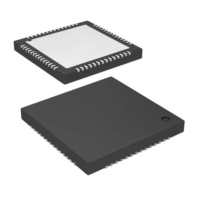
Infineon Technologies CY7C68000A-56LFXC
- Part No.:
- CY7C68000A-56LFXC
- Manufacturer:
- Infineon Technologies
- Category:
- Drivers, Receivers, Transceivers
- Package:
- 56-VFQFN Exposed Pad
- Datasheet:
-
 CY7C68000A-56LFXC.pdf
- Description:
- IC TRANSCEIVER FULL 1/1 56QFN
- Quantity:
- Payment:

- Shipping:

Inventory:4,831
Please send an inquiry. Send us your inquiry, and we will respond immediately.
Product details
Overview
CY7C68000A-56LFXC from Cypress Semiconductor is a USB 2.0 UTMI-compliant transceiver IC implementing physical-layer serialization/deserialization between USB differential signaling (DPLUS/DMINUS) and parallel host interface. It supports both High Speed (480 Mbps) and Full Speed (12 Mbps) modes, integrates internal 1.5 kΩ DPLUS pull-up and on-die impedance termination, and operates from a 24 MHz crystal with on-chip PLL generating 30 MHz (16-bit bus) or 60 MHz (8-bit bus) clock. Used in mobile handsets interfacing Intel Monahans processors.
For engineers reviewing the CY7C68000A-56LFXC datasheet, CY7C68000A-56LFXC pinout, CY7C68000A-56LFXC application, or CY7C68000A-56LFXC equivalent, key selection criteria include UTMI v1.05 compliance, tristate-enabled shared-bus operation, integrated analog termination, synchronous field/EOP detection/generation, and dual-speed (HS/FS) transceiver switching via XcvrSelect/TermSelect pins.
Technical Context
The CY7C68000A implements a full UTMI+ Level 1–compliant PHY layer with dedicated HS and FS transceiver paths selected by XcvrSelect and termination control via TermSelect. Its internal PLL locks to a 24 MHz ±100 ppm crystal to generate precise 30 MHz (16-bit mode) or 60 MHz (8-bit mode) parallel interface clocks synchronized to USB packet boundaries.
It performs real-time bit stuffing/unstuffing and NRZI encoding/decoding, detects SE0, J/K states via LineState[1:0], and provides synchronous EOP/SYNC assertion timing relative to TXValid/RXValid. Operational modes (OpMode[1:0]) enable soft disconnect, disable encoding, or normal USB protocol handling without external logic.
Key Specifications
| Parameter | Value and Actual Design Meaning |
|---|---|
| USB Speed Modes | High Speed (480 Mbps) and Full Speed (12 Mbps); no Low Speed support |
| UTMI Compliance | UTMI+ Level 1 v1.05 compliant; certified for USB 2.0 device operation |
| Parallel Interface | Configurable 8-bit bidirectional @ 60 MHz or 16-bit bidirectional @ 30 MHz |
| Crystal Input | 24 MHz ±100 ppm parallel-resonant fundamental-mode crystal required |
| Supply Voltage | 3.3 V nominal; separate AVCC/AGND for analog section; digital I/O tolerant |
| Integrated Termination | Internal 1.5 kΩ DPLUS pull-up and USB data line impedance matching; no external resistors needed |
| Power Management | Suspend mode reduces current; Tri_state enabled only during Suspend to share UTMI bus |
Pinout & Package
Package: 56-pin QFN (7 mm × 7 mm, 0.5 mm pitch), RoHS-compliant, thermally enhanced with exposed pad.
| Pin | Circuit Role | Design Meaning |
|---|---|---|
| D0–D15 | Bidirectional Data Bus | 16-bit parallel interface; D0–D7 used in 8-bit mode; D8–D15 active only in 16-bit mode per DataBus16_8 |
| CLK | Output Clock | 30 MHz (16-bit) or 60 MHz (8-bit) synchronous clock for data capture; derived from internal PLL |
| XcvrSelect / TermSelect | Input Control | XcvrSelect = 0 selects HS transceiver; TermSelect = 0 enables HS termination (SE0 assertion) |
| Suspend / Tri_state | Input Control | Suspend activates low-power state; Tri_state (only active during Suspend) tristates all I/Os for bus sharing |
| DPLUS / DMINUS | USB Differential I/O | Direct connection to USB cable; internal termination eliminates need for external 90 Ω differential or 1.5 kΩ pull-up |
| LineState[1:0] | Output Status | Combinatorial then CLK-synchronized reflection of DMINUS/DPLUS states (00=SE0, 01=J, 10=K, 11=SE1) |
| TXValid / RXValid | Handshake Control | TXValid initiates SYNC; negation triggers EOP; RXValid indicates valid receive data ready for latching |
Key Features
| Feature | Design Value |
|---|---|
| UTMI+ Level 1 Compliance | Fully implements Transceiver Macrocell Interface v1.05 for seamless integration with USB 2.0 controllers |
| Integrated Analog Termination | On-die 1.5 kΩ DPLUS pull-up and matched USB line impedance reduce BOM count and layout sensitivity |
| Dynamic Bus Sharing | Tristate mode activated only during Suspend enables multiplexing of UTMI bus among multiple peripherals |
| Dual-Speed Transceiver Switching | Hardware-selectable HS/FS paths via XcvrSelect and TermSelect allow runtime speed negotiation without firmware overhead |
| Synchronous Packet Boundary Handling | Hardware-detected SYNC/EOP and field alignment ensure deterministic timing for high-reliability streaming applications |
Applications
| Smartphone Baseband Interface | Intel Monahans Processor Companion |
|---|---|
Use Scenario: Integrated into smartphone baseband SoCs to provide USB 2.0 device connectivity for PC synchronization, charging, and peripheral attachment. IC Role / Device Role / Timing Role: USB 2.0 PHY transceiver handling physical layer serialization, clock recovery, and differential signaling conversion. Use Value: Enables HS/FS mode switching per host request while maintaining <50 ns tristate response for GPIO-constrained handset designs. | Use Scenario: Paired with Intel Monahans-P/L application processors to deliver certified USB 2.0 device functionality in PDA phones and media players. IC Role / Device Role / Timing Role: UTMI-compliant PHY providing synchronous 16-bit/30 MHz or 8-bit/60 MHz parallel interface to processor's USB controller. Use Value: Eliminates need for external termination resistors and reduces PCB area by 25% versus discrete PHY solutions. |
| Portable Media Player Docking | DSL Modem USB Device Port |
Use Scenario: Embedded in portable media players to support high-bandwidth file transfer and firmware updates via USB docking stations. IC Role / Device Role / Timing Role: High-speed serial-to-parallel converter managing bit stuffing, NRZI decoding, and EOP detection for error-free bulk transfers. Use Value: Achieves sustained 480 Mbps throughput with hardware-accelerated packet boundary detection and staging register buffering. | Use Scenario: Used in DSL modems to implement USB 2.0 device port for configuration, diagnostics, and firmware download from host PCs. IC Role / Device Role / Timing Role: Full-speed and high-speed transceiver supporting USB reset/suspend/resume detection and resume signaling generation. Use Value: Reduces power consumption by >70% in Suspend mode while retaining ability to detect upstream resume within 200 μs of wake signal. |
Equivalent & Alternatives
The following parts are listed as comparable options for similar USB 2.0 UTMI transceiver applications.
| Alternative Part | Technical Difference | Application Difference | Selection Advice |
|---|---|---|---|
| ISP1507A | Single 3.3 V supply; no internal crystal oscillator; requires external 48 MHz clock or PLL | Lacks integrated 24 MHz crystal interface and PLL; needs external clock source | Select when system already provides 48 MHz clock and board space for external oscillator is constrained |
| USB3300 | Supports OTG; includes integrated USB switch; higher ESD rating (±15 kV HBM) | Enables dual-role device operation; adds USB switch control logic not present in CY7C68000A | Select when OTG capability or enhanced ESD protection is required beyond USB 2.0 device-only operation |
Compared with ISP1507A and USB3300, the CY7C68000A offers tighter integration of crystal oscillator + PLL + termination, lower pin count for QFN/VFBGA packages, and optimized timing for Intel Monahans interfaces-making it preferred for cost-sensitive, space-constrained mobile device PHY implementations where OTG is not needed.
Availability
CY7C68000A-56LFXC is available at Aetrix Electronics and suitable for smartphone baseband interfaces, Intel Monahans companion designs, and portable media player docking systems requiring stable component supply and long-term lifecycle support.
Supply support for CY7C68000A-56LFXC includes scheduled delivery planning, volume procurement assistance, BOM continuity management, traceable sourcing, and lifecycle availability coordination for OEM customers, industrial embedded developers, connected-device designers, and electronics production programs.
Manufacturer
Cypress Semiconductor (now part of Infineon Technologies) is a fabless semiconductor company specializing in programmable system-on-chip (PSoC), memory, and USB connectivity solutions for embedded systems.
The MoBL-USB™ TX2 product line was designed specifically to deliver compact, low-power, UTMI-compliant USB 2.0 PHYs for mobile and handheld applications where board space, power efficiency, and integration density are critical.
FAQ
What is the function of the Tri_state pin, and when must it be asserted?
The Tri_state pin places all I/Os and outputs into high-impedance state, enabling shared use of the UTMI bus with other devices. It can only be asserted while the device is in Suspend mode (Suspend = LOW). Assertion occurs within ~50 ns, and deassertion restores drive strength in ~50 ns. Leaving inputs floating during Tri_state is prohibited.
Does CY7C68000A-56LFXC require external termination resistors for USB data lines?
No. The CY7C68000A-56LFXC integrates all required USB 2.0 terminations: internal 1.5 kΩ pull-up on DPLUS and precisely trimmed differential impedance matching on DPLUS/DMINUS. External resistors are unnecessary and would violate USB specification compliance.
How does the device handle clock generation for the parallel interface?
The device uses an on-chip PLL locked to an external 24 MHz ±100 ppm crystal (connected to XTALIN/XTALOUT) to generate either 30 MHz (for 16-bit mode) or 60 MHz (for 8-bit mode) parallel interface clock. The DataBus16_8 pin selects the mode and corresponding clock frequency at power-on reset.
Can CY7C68000A-56LFXC operate in Low Speed (1.5 Mbps) USB mode?
No. The CY7C68000A-56LFXC supports only Full Speed (12 Mbps) and High Speed (480 Mbps) USB 2.0 modes. It explicitly excludes Low Speed operation per its functional specification and pin-level timing requirements.
CY7C68000A-56LFXC Specifications
- Product attributes
- Attribute value
- Manufacturer:
- Infineon Technologies
- Series:
- CY7C
- Package/Case:
- 56-VFQFN Exposed Pad
- Packaging:
- Tray
- Product Status:
- Obsolete
- Type:
- Transceiver
- Protocol:
- USB 2.0
- Number of Drivers/Receivers:
- 1/1
- Duplex:
- Full
- Receiver Hysteresis:
- -
- Data Rate:
- -
- Voltage - Supply:
- 3V ~ 3.6V
- Operating Temperature:
- 0°C ~ 70°C
- Grade:
- -
- Qualification:
- -
- Mounting Type:
- Surface Mount
- Supplier Device Package:
- 56-QFN (8x8)
CY7C68000A-56LFXC FAQ
1.How can I place an order for CY7C68000A-56LFXC through Aetrix?
Please submit a Request for Quotation (RFQ) for CY7C68000A-56LFXC on Aetrix. Our sales agent will provide a competitive quotation and guide you through the order confirmation once you accept the terms.
2.Are the price and stock information for CY7C68000A-56LFXC reliable?
The price and inventory of CY7C68000A-56LFXC are updated periodically and may fluctuate due to market conditions. Stock and pricing data are typically refreshed every 24 hours. Quotation validity for CY7C68000A-56LFXC is usually 5 days.
3.What payment methods are accepted for CY7C68000A-56LFXC?
We accept Wire Transfer, PayPal, Credit Card, Western Union, MoneyGram, and Escrow for CY7C68000A-56LFXC transactions.
Note: Certain payment methods may incur a processing fee.
4.How is shipping managed for CY7C68000A-56LFXC?
CY7C68000A-56LFXC orders can be shipped via leading logistics carriers, including DHL, UPS, FedEx, TNT, or Registered Mail.
Once your CY7C68000A-56LFXC order is processed, you will receive an email with the shipment details and tracking number.
Note: Tracking information may take up to 24 hours to appear. Express delivery typically takes 3–5 business days.
5.How can I obtain technical support or documentation for CY7C68000A-56LFXC?
For technical support, including CY7C68000A-56LFXC datasheets, pinout diagrams, or application guidance, please contact our engineering support team. They can provide detailed documentation and assistance for your CY7C68000A-56LFXC requirements.
6.How does Aetrix verify that CY7C68000A-56LFXC is sourced from the original manufacturer or authorized distributors?
All CY7C68000A-56LFXC products on Aetrix are procured from qualified distributors and authorized channels. Our dedicated quality assurance team conducts strict verification, including traceability checks and, if necessary, third-party testing. This ensures that CY7C68000A-56LFXC meets industry standards.
7.What is the process for return or replacement of CY7C68000A-56LFXC?
All CY7C68000A-56LFXC units undergo pre-shipment inspection (PSI). If there is an issue with CY7C68000A-56LFXC, returns or replacements are accepted under the following conditions:
1.Quantity discrepancies, incorrect items, or visible external defects (such as breakage or corrosion), acknowledged by Aetrix.
2.The issue is reported within 90 days of delivery.
3.The CY7C68000A-56LFXC part is unused and in its original packaging.
Return procedure for CY7C68000A-56LFXC:
1.Submit a request within 90 days.
2.Obtain a Return Material Authorization (RMA) from Aetrix.
CY7C68000A-56LFXC Tags

-
ATA6561-GAQW-N
Microchip Technology
-
ATA6561-GBQW-N
Microchip Technology

-
AM26LS32ACDR
Texas Instruments

-
SP485CN-L/TR
MaxLinear, Inc.
-
SP485EN-L/TR
MaxLinear, Inc.
-
SP485EEN-L/TR
MaxLinear, Inc.
-
SP485ECN-L/TR
MaxLinear, Inc.
-
THVD1400DR
Texas Instruments
-
AM26C31IDR
Texas Instruments

-
TLIN1021ADRQ1
Texas Instruments
-
MAX232IDR
Texas Instruments
-
AM26C32IDR
Texas Instruments
Tech Hub

LDO regulator guide covering low dropout voltage, power dissipation, thermal design, PSRR, output noise, capacitor stability, adjustable LDO circuits, LDO vs buck converter and datasheet selection chec…

Conditional Access Module guide covering CAM meaning, CI/CI+ interface, smart card authorization, DVB security workflow, TV and set-top box compatibility, internal electronics, ESD protection, connecto…

Guide to electronic component obsolescence covering EOL risk, PCN/PDN notices, last-time buy planning, replacement options, form-fit-function validation, counterfeit risk and BOM lifecycle management.

18650 battery guide covering lithium-ion cell basics, 3.6V/3.7V voltage, 4.2V charging, mAh and Wh capacity, protected cells, chargers, BMS, series-parallel packs, holders, welding and sourcing checks.…

Hall effect sensor guide covering working principle, linear and digital sensors, Arduino circuits, current sensing, speed detection, automotive applications, A3144 examples, signal filtering and datash…

Product Change Notification guide for electronic components, covering PCN meaning, PCN vs PDN/EOL, common change types, risk levels, form-fit-function review, engineering validation, BOM control, LTB/L…

A practical guide to blend door actuators, covering HVAC function, symptoms, location, AC and heater issues, reset and calibration, replacement cost, electrical diagnosis, compatibility checks, and rep…

Engineering guide to Raspberry Pi alternatives, covering chip-level differences, Orange Pi, ROCK, Jetson, Banana Pi, NanoPi, Compute Module, Pico, GPIO, camera, HAT compatibility, and replacement risks…

Engineering guide to dynamic load response testing for high-current buck converters, covering load step setup, slew rate, Vcore undershoot, overshoot, recovery time, probe location, output capacitors a…

Engineering guide to output capacitor selection for ASIC Vcore rails, covering bulk capacitors, polymer capacitors, MLCC decoupling, DC bias, ESR, ESL, placement, transient response and substitution ri…


