
 My Inquiry
 My Account


Infineon Technologies CY7C68003-20FNXIT
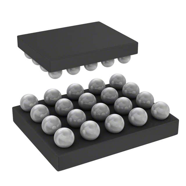
- Part No.:
- CY7C68003-20FNXIT
- Manufacturer:
- Infineon Technologies
- Category:
- Drivers, Receivers, Transceivers
- Package:
- 20-UFBGA, WLCSP
- Datasheet:
-
 CY7C68003-20FNXIT.pdf
- Description:
- IC TRANSCEIVER FULL 1/1 20WLCSP
- Quantity:
- Payment:

- Shipping:

Inventory:3,556
Please send an inquiry. Send us your inquiry, and we will respond immediately.
Product details
Overview
CY7C68003-20FNXIT from Cypress Semiconductor is a USB 2.0 ULPI transceiver supporting Full Speed and High Speed modes, featuring integrated PLL (13/19.2/24/26 MHz), on-chip oscillator, and 1.8 V core supply with 1.8–3.3 V I/O voltage range. It implements UTMI+ Level 0 interface, supports UART pass-through mode, and operates across –40 °C to +85 °C in a 2.14 × 1.76 mm 20-pin WLCSP package for mobile handset applications.
For engineers reviewing the CY7C68003-20FNXIT datasheet, CY7C68003-20FNXIT pinout, CY7C68003-20FNXIT application, or CY7C68003-20FNXIT equivalent, key selection criteria include ULPI SDR 8-bit interface compliance, integrated termination/pull-up resistors, sleep-mode current (5 µA), VBATT input range (3.0–5.775 V), and industrial temperature operation.
Technical Context
The CY7C68003-20FNXIT implements a UTMI+ Level 0-compliant USB 2.0 PHY with dedicated ULPI link interface, enabling direct connection to host/device controllers without external level-shifting or timing compensation. Its internal PLL locks to 13/19.2/24/26 MHz reference inputs and generates precise 480 MHz HS clock with fractional multiplication.
It integrates USB FS/HS analog front-end with on-die 1.5 kΩ pull-up resistor on DP, 15 kΩ termination on DP/DM, and supports Carkit UART pass-through via DP/DM signal remapping to DATA[1:0]. Power domains are isolated: VCC (1.7–1.9 V), VIO (1.7–3.6 V), and VBATT (3.0–5.775 V).
Key Specifications
| Parameter | Value and Actual Design Meaning |
|---|---|
| USB Compliance | Full Speed (12 Mbps) and High Speed (480 Mbps) compliant per USB 2.0 specification. |
| ULPI Interface | 8-bit SDR data path, UTMI+ Level 0 compatible, supports multi-voltage I/O (1.8–3.3 V). |
| Reference Clock | 13 / 19.2 / 24 / 26 MHz crystal or LVCMOS input; PLL generates stable 480 MHz HS clock. |
| Power Consumption | 5 µA nominal in sleep mode; 30 mA nominal during active HS transfer. |
| Operating Temperature | –40 °C to +85 °C industrial grade, validated for mobile handset thermal profiles. |
| ESD Protection | JESD22-A114D 8 kV HBM on DP/DM/VSS; IEC61000-4-2 8 kV contact / 15 kV air discharge. |
| VBATT Input Range | 3.0 V to 5.775 V direct battery input, powers internal 3.3 V regulator for USBIO/XOSC blocks. |
Pinout & Package
Package: 20-pin Wafer-Level Chip Scale Package (WLCSP), 2.14 × 1.76 mm, 0.4 mm pitch, bottom-side solder balls.
| Pin/Terminal | Circuit Role | Design Meaning |
|---|---|---|
| DP / DM | USB differential data pair | Direct connection to USB receptacle; includes integrated 15 kΩ termination and 1.5 kΩ DP pull-up. |
| VCC | Core power supply | 1.7–1.9 V supply for digital logic and PLL; requires local 100 nF decoupling. |
| VIO | I/O voltage reference | Configures ULPI interface voltage level (1.8–3.3 V); sets LVCMOS signaling threshold. |
| VBATT | Battery input | 3.0–5.775 V input powering internal 3.3 V regulator for analog/oscillator blocks. |
| RESET_N | Active-low reset/control | Triple-function pin: reset, enter sleep mode (with tSTATE low), or enter configuration mode. |
| DATA[7:0] | ULPI bidirectional data bus | 8-bit SDR interface for register access and command/data exchange with UTMI+ controller. |
| CLOCK / DIR / STP / NXT | ULPI control signals | Standard ULPI handshake lines; support synchronous command/response protocol at up to 60 MHz. |
| XI / XO | Clock input/output | Crystal connection pins (parallel resonant, 13/19.2/24/26 MHz); XO not bonded in 20-pin WLCSP. |
Key Features
| Feature | Design Value |
|---|---|
| Integrated USB termination & pull-up | Eliminates 4 external resistors (15 kΩ DP/DM termination + 1.5 kΩ DP pull-up), reducing BOM count and PCB area. |
| Multi-range I/O voltage (1.8–3.3 V) | Enables direct interfacing with diverse UTMI+ controllers without external level shifters or voltage translators. |
| UART pass-through mode | Reuses DP/DM pins as UART TXD/RXD (via DATA[0]/DATA[1]), enabling car-kit accessory communication over USB connector. |
| Low-power sleep mode (5 µA) | Supports battery-sensitive mobile designs by minimizing quiescent current during USB suspend states. |
| On-chip oscillator + PLL | Removes need for external clock generator; supports crystal or LVCMOS clock source with auto-frequency detection. |
Applications
| Mobile Handset Connectivity | Portable Media Player (PMP) USB Interface |
|---|---|
|
Use Scenario: Integration into smartphone baseband SoC subsystem for USB device-mode connectivity to PC or charger. IC Role / Device Role / Timing Role: USB 2.0 PHY transceiver handling analog signaling, impedance matching, and clock recovery for HS/FS operation. Use Value: Enables compact layout with integrated termination/pull-up and ultra-low sleep current (5 µA), extending battery life during idle USB states. |
Use Scenario: USB device interface in flash-based audio/video players requiring high-speed file transfer and charging. IC Role / Device Role / Timing Role: UTMI+ Level 0 PHY bridging SoC's digital USB controller to physical USB port with minimal latency. Use Value: Supports 480 Mbps HS transfers while maintaining <30 mA active current and industrial temperature operation (–40 °C to +85 °C). |
| DTV Set-Top Box Peripheral Interface | Portable GPS Navigation Unit |
|
Use Scenario: Adding USB device functionality (e.g., firmware update, content import) to digital TV receivers. IC Role / Device Role / Timing Role: USB transceiver providing robust ESD protection (8 kV HBM, 15 kV air) for consumer-facing USB ports. Use Value: Integrated IEC61000-4-2 compliant ESD protection eliminates need for external TVS diodes on DP/DM lines. |
Use Scenario: Enabling USB device-mode connection between GPS unit and host PC for map updates and track logging. IC Role / Device Role / Timing Role: Low-power USB PHY supporting both standard USB data transfer and Carkit UART pass-through over same DP/DM pins. Use Value: Dual-mode capability allows single USB connector to serve both data sync and vehicle hands-free UART communication. |
Equivalent & Alternatives
The following parts are listed as comparable options for similar USB 2.0 ULPI transceiver applications.
| Alternative Part | Technical Difference | Application Difference | Selection Advice |
|---|---|---|---|
| SMSC USB3317C-EZK | Supports UTMI+ Level 1; includes integrated USB switch and VBUS detection; no UART pass-through mode. | Targeted at embedded host applications with dual-role capability; lacks Carkit mode and WLCSP option. | Choose when UTMI+ Level 1 features or VBUS sensing are required; not drop-in for CY7C68003-20FNXIT's WLCSP footprint. |
| Microchip USB2502-AEZG | USB 2.0 hub controller (not transceiver); integrates PHY + link layer; requires external crystal only at 12/24 MHz. | Designed for multi-port hub systems; not suitable as standalone PHY replacement. | Select only for hub-based architectures; incompatible as direct CY7C68003-20FNXIT functional substitute. |
Compared with SMSC USB3317C-EZK and Microchip USB2502-AEZG, the CY7C68003-20FNXIT uniquely combines WLCSP packaging, UART pass-through, and 5 µA sleep current-making it optimal for space-constrained, battery-powered USB device endpoints where dual-mode serial communication is needed.
Availability
CY7C68003-20FNXIT is available at Aetrix Electronics and suitable for mobile handsets, portable media players, and portable GPS units requiring stable component supply, industrial temperature operation, and low-power USB device connectivity.
Supply support for CY7C68003-20FNXIT includes scheduled delivery planning, volume procurement assistance, BOM continuity management, traceable sourcing, and lifecycle availability coordination for OEM customers, industrial embedded developers, connected-device designers, and electronics production programs.
Manufacturer
Cypress Semiconductor (now part of Infineon Technologies) designs high-performance mixed-signal ICs for embedded connectivity, memory, and programmable systems.
The MoBL-USB™ TX2UL product line targets mobile and portable electronics, delivering compact, low-power USB 2.0 PHY solutions with integrated clocking, termination, and advanced operational modes like UART pass-through.
FAQ
What is the function of the RESET_N pin on CY7C68003-20FNXIT?
The RESET_N pin serves three distinct functions: asserting it for tSTATE places the device into Sleep Mode; asserting it during power-on initiates Configuration Mode; and deasserting it exits Configuration Mode. When unused, it must be pulled high to ensure normal operation. All ULPI interface pins are tristated during Sleep and Configuration Modes.
Does CY7C68003-20FNXIT support USB host mode?
No. The CY7C68003-20FNXIT supports USB device mode only, as confirmed in its official documentation. It implements UTMI+ Level 0 for device-side PHY functionality and lacks host-side signaling logic, VBUS sensing, or OTG capability. It must be paired with a UTMI+-compliant USB device controller.
Can the CY7C68003-20FNXIT operate without an external crystal?
Yes - it accepts either a 13/19.2/24/26 MHz crystal across XI/XO or a single-ended LVCMOS clock applied to XI. The XO pin is not bonded in the 20-pin WLCSP package, so crystal operation requires proper load capacitance (12 pF ±5%) and trace layout per Figure 2 in the datasheet. External clock input bypasses the oscillator circuit.
What is the purpose of UART pass-through mode?
UART pass-through mode repurposes DP and DM pins as UART TXD and RXD using DATA[0] and DATA[1] under software control (Carkit Mode bit in Interface Control Register). This enables car-kit accessories to communicate over the same USB connector without additional wiring, with automatic clock gating to reduce power during UART operation.
CY7C68003-20FNXIT Specifications
- Product attributes
- Attribute value
- Manufacturer:
- Infineon Technologies
- Series:
- CY7C
- Package/Case:
- 20-UFBGA, WLCSP
- Packaging:
- Tape & Reel (TR)
- Product Status:
- Obsolete
- Type:
- Transceiver
- Protocol:
- USB 2.0
- Number of Drivers/Receivers:
- 1/1
- Duplex:
- Full
- Receiver Hysteresis:
- -
- Data Rate:
- -
- Voltage - Supply:
- 1.8V ~ 3.3V
- Operating Temperature:
- -40°C ~ 85°C
- Grade:
- -
- Qualification:
- -
- Mounting Type:
- Surface Mount
- Supplier Device Package:
- 20-WLCSP (2.14x1.76)
CY7C68003-20FNXIT FAQ
1.How can I place an order for CY7C68003-20FNXIT through Aetrix?
Please submit a Request for Quotation (RFQ) for CY7C68003-20FNXIT on Aetrix. Our sales agent will provide a competitive quotation and guide you through the order confirmation once you accept the terms.
2.Are the price and stock information for CY7C68003-20FNXIT reliable?
The price and inventory of CY7C68003-20FNXIT are updated periodically and may fluctuate due to market conditions. Stock and pricing data are typically refreshed every 24 hours. Quotation validity for CY7C68003-20FNXIT is usually 5 days.
3.What payment methods are accepted for CY7C68003-20FNXIT?
We accept Wire Transfer, PayPal, Credit Card, Western Union, MoneyGram, and Escrow for CY7C68003-20FNXIT transactions.
Note: Certain payment methods may incur a processing fee.
4.How is shipping managed for CY7C68003-20FNXIT?
CY7C68003-20FNXIT orders can be shipped via leading logistics carriers, including DHL, UPS, FedEx, TNT, or Registered Mail.
Once your CY7C68003-20FNXIT order is processed, you will receive an email with the shipment details and tracking number.
Note: Tracking information may take up to 24 hours to appear. Express delivery typically takes 3–5 business days.
5.How can I obtain technical support or documentation for CY7C68003-20FNXIT?
For technical support, including CY7C68003-20FNXIT datasheets, pinout diagrams, or application guidance, please contact our engineering support team. They can provide detailed documentation and assistance for your CY7C68003-20FNXIT requirements.
6.How does Aetrix verify that CY7C68003-20FNXIT is sourced from the original manufacturer or authorized distributors?
All CY7C68003-20FNXIT products on Aetrix are procured from qualified distributors and authorized channels. Our dedicated quality assurance team conducts strict verification, including traceability checks and, if necessary, third-party testing. This ensures that CY7C68003-20FNXIT meets industry standards.
7.What is the process for return or replacement of CY7C68003-20FNXIT?
All CY7C68003-20FNXIT units undergo pre-shipment inspection (PSI). If there is an issue with CY7C68003-20FNXIT, returns or replacements are accepted under the following conditions:
1.Quantity discrepancies, incorrect items, or visible external defects (such as breakage or corrosion), acknowledged by Aetrix.
2.The issue is reported within 90 days of delivery.
3.The CY7C68003-20FNXIT part is unused and in its original packaging.
Return procedure for CY7C68003-20FNXIT:
1.Submit a request within 90 days.
2.Obtain a Return Material Authorization (RMA) from Aetrix.
CY7C68003-20FNXIT Tags

-
ATA6561-GAQW-N
Microchip Technology
-
ATA6561-GBQW-N
Microchip Technology

-
AM26LS32ACDR
Texas Instruments

-
SP485CN-L/TR
MaxLinear, Inc.
-
SP485EN-L/TR
MaxLinear, Inc.
-
SP485EEN-L/TR
MaxLinear, Inc.
-
SP485ECN-L/TR
MaxLinear, Inc.
-
THVD1400DR
Texas Instruments
-
AM26C31IDR
Texas Instruments

-
TLIN1021ADRQ1
Texas Instruments
-
MAX232IDR
Texas Instruments
-
AM26C32IDR
Texas Instruments
Tech Hub

LDO regulator guide covering low dropout voltage, power dissipation, thermal design, PSRR, output noise, capacitor stability, adjustable LDO circuits, LDO vs buck converter and datasheet selection chec…

Conditional Access Module guide covering CAM meaning, CI/CI+ interface, smart card authorization, DVB security workflow, TV and set-top box compatibility, internal electronics, ESD protection, connecto…

Guide to electronic component obsolescence covering EOL risk, PCN/PDN notices, last-time buy planning, replacement options, form-fit-function validation, counterfeit risk and BOM lifecycle management.

18650 battery guide covering lithium-ion cell basics, 3.6V/3.7V voltage, 4.2V charging, mAh and Wh capacity, protected cells, chargers, BMS, series-parallel packs, holders, welding and sourcing checks.…

Hall effect sensor guide covering working principle, linear and digital sensors, Arduino circuits, current sensing, speed detection, automotive applications, A3144 examples, signal filtering and datash…

Product Change Notification guide for electronic components, covering PCN meaning, PCN vs PDN/EOL, common change types, risk levels, form-fit-function review, engineering validation, BOM control, LTB/L…

A practical guide to blend door actuators, covering HVAC function, symptoms, location, AC and heater issues, reset and calibration, replacement cost, electrical diagnosis, compatibility checks, and rep…

Engineering guide to Raspberry Pi alternatives, covering chip-level differences, Orange Pi, ROCK, Jetson, Banana Pi, NanoPi, Compute Module, Pico, GPIO, camera, HAT compatibility, and replacement risks…

Engineering guide to dynamic load response testing for high-current buck converters, covering load step setup, slew rate, Vcore undershoot, overshoot, recovery time, probe location, output capacitors a…

Engineering guide to output capacitor selection for ASIC Vcore rails, covering bulk capacitors, polymer capacitors, MLCC decoupling, DC bias, ESR, ESL, placement, transient response and substitution ri…


