
 My Inquiry
 My Account


Infineon Technologies CY7C68013A-56LTXI
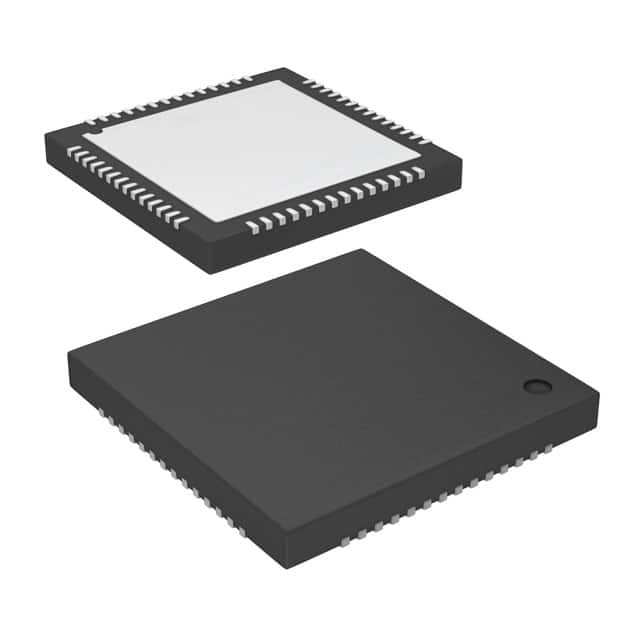
- Part No.:
- CY7C68013A-56LTXI
- Manufacturer:
- Infineon Technologies
- Category:
- Application Specific Microcontrollers
- Package:
- 56-VFQFN Exposed Pad
- Datasheet:
-
 CY7C68013A-56LTXI.pdf
- Description:
- IC MCU USB PHERIPH FX2LP 56VQFN
- Quantity:
- Payment:

- Shipping:

Inventory:1,659
Please send an inquiry. Send us your inquiry, and we will respond immediately.
Product details
Overview
CY7C68013A-56LTXI from Infineon Technologies (formerly Cypress Semiconductor) is a high-speed USB 2.0 peripheral controller integrating a USB 2.0 transceiver, Smart Serial Interface Engine (SIE), enhanced 8051 microcontroller, and General Programmable Interface (GPIF) in a single 56-pin QFN package. It delivers up to 53 MB/s data throughput, supports 48/24/12 MHz CPU operation, includes 16 KB on-chip RAM, and targets bus-powered USB peripheral designs such as video capture dongles and memory card readers.
For engineers reviewing the CY7C68013A-56LTXI datasheet, CY7C68013A-56LTXI pinout, CY7C68013A-56LTXI application, or CY7C68013A-56LTXI equivalent, key selection criteria include suspend current (300 µA typ), GPIF waveform programmability, endpoint buffering options (double/triple/quad), and compatibility with legacy FX2 firmware and hardware layouts.
Technical Context
The CY7C68013A implements a hardware-accelerated USB 2.0 protocol stack via its Smart SIE, offloading enumeration, token handling, and CRC generation from the 8051 core. Its PLL-derived 480 MHz PHY clock enables Hi-Speed (480 Mbps) signaling while the 8051 runs at configurable 12/24/48 MHz using four clocks per instruction cycle.
GPIF operates independently of the CPU, supporting programmable 8-/16-bit parallel waveforms with up to six RDY inputs and six CTL outputs. Four integrated FIFOs-each configurable as master or slave-enable glueless interfacing to ATA, EPP, PCMCIA, or FPGA logic without external address latches or control logic.
Key Specifications
| Parameter | Value and Actual Design Meaning |
|---|---|
| USB Speed | Hi-Speed (480 Mbps) and Full-Speed (12 Mbps); no Low-Speed support - enables direct connection to USB 2.0 hosts without hub translation. |
| CPU Core | Enhanced 8051 running at 12/24/48 MHz - retains full object-code compatibility with legacy FX2 firmware while delivering higher throughput. |
| On-Chip RAM | 16 KB code/data RAM - sufficient for complex USB descriptors, endpoint buffers, and application logic without external memory. |
| Suspend Current | 300 µA (typ) - meets USB bus-powered suspend requirements for portable devices like scanners and camcorders. |
| Endpoints | Four programmable BULK/INTERRUPT/ISOCHRONOUS endpoints + one additional 64-byte BULK/INTERRUPT endpoint - supports concurrent high-bandwidth streaming and low-latency control transfers. |
| GPIF Bus Width | 8-bit or 16-bit programmable interface - allows direct connection to SRAM, FPGA, or ASIC without glue logic or address demultiplexing. |
| I²C Controller | Integrated 100/400 kHz I²C master - used for EEPROM configuration, sensor communication, or power management IC control without CPU overhead. |
Pinout & Package
Package: 56-pin QFN (7 mm × 7 mm, 0.5 mm pitch), RoHS-compliant, industrial temperature grade (–40°C to +85°C).
| Pin/Terminal | Circuit Role | Design Meaning |
|---|---|---|
| D+ / D− | USB 2.0 differential data pair | Direct connection to USB connector; internal 1.5 kΩ pull-up on D+ enables device enumeration without external resistor. |
| CLKOUT | 8051 clock output | Configurable 12/24/48 MHz square wave; three-state and invertible - used for synchronizing external logic or debugging clock domain alignment. |
| SLCS# | Slave FIFO chip select | Active-low enable for Slave FIFO mode; when asserted, data bus (FD0–FD7) and control signals (SLRD#, SLWR#, PKTEND#) become active. |
| FLAGA / FLAGB | FIFO status indicators | Programmable flags indicating FIFO full/empty/almost-full - used for handshaking with external controllers without polling or interrupts. |
| CTL0–CTL5 | GPIF control outputs | Configurable GPIOs driven by GPIF state machine - generate custom strobes, chip selects, or bus control signals synchronized to data transfer. |
| RDY0–RDY5 | GPIF ready inputs | External handshake signals accepted by GPIF - pause waveform execution until external device asserts readiness, enabling adaptive timing. |
Key Features
| Feature | Design Value |
|---|---|
| Smart SIE | Hardware USB protocol engine handles token, handshake, and CRC generation - reduces 8051 firmware size and eliminates USB compliance risk from software stack bugs. |
| GPIF Waveform Descriptors | Up to 16-state, 8-/16-bit programmable interface - defines precise timing for read/write strobes, address setup, and control signals without CPU intervention. |
| Slave FIFO Mode | 8-bit asynchronous interface with auto-incrementing address and packet-end strobe - enables simple DMA-like data pumping from FPGA or DSP with minimal firmware overhead. |
| Boot Sources | Firmware loaded from USB, internal RAM, or external EEPROM - supports field-upgradable devices and secure boot via encrypted EEPROM image. |
| Integrated I²C Master | 100/400 kHz operation with automatic ACK/NACK handling - manages configuration EEPROM, temperature sensors, or PMIC registers without bit-banging. |
Applications
| Portable Video Capture Dongle | USB-to-ATA Bridge |
|---|---|
Use Scenario: Real-time HDMI-to-USB video capture for live streaming or recording on host PCs. IC Role / Device Role / Timing Role: USB peripheral controller managing high-bandwidth isochronous transfers and GPIF-driven video pixel ingestion from HDMI receiver ASIC. Use Value: Achieves sustained 40+ MB/s throughput using quad-buffered ISOCHRONOUS endpoints and GPIF waveform synchronized to pixel clock. |
Use Scenario: Converting legacy PATA hard drives into USB 2.0 external storage units. IC Role / Device Role / Timing Role: Protocol translator bridging ATA command set to USB mass storage class via Slave FIFO and embedded 8051 command parser. Use Value: Eliminates need for external FIFO or CPLD by leveraging integrated 4× FIFOs and ATA timing control via GPIF descriptor states. |
| Industrial Barcode Scanner | Medical Imaging Data Logger |
Use Scenario: Battery-powered handheld scanner transmitting decoded barcode strings over USB to POS terminals. IC Role / Device Role / Timing Role: Low-power USB peripheral with suspend/resume handling and UART-to-USB conversion via 8051 USART and BULK endpoints. Use Value: 300 µA typical suspend current extends battery life; built-in USB transceiver removes external PHY cost and layout complexity. |
Use Scenario: Capturing time-stamped ECG or ultrasound frames from analog front-end and storing to USB flash drive. IC Role / Device Role / Timing Role: High-reliability data aggregator using dual USARTs (one for sensor sync, one for debug), ECC-enabled memory card interface, and interrupt-driven bulk transfers. Use Value: Smart SIE ensures deterministic USB response under variable load; on-chip RAM buffers transient bursts during flash write latency. |
Equivalent & Alternatives
The following parts are listed as comparable options for similar USB peripheral controller applications.
| Alternative Part | Technical Difference | Application Difference | Selection Advice |
|---|---|---|---|
| CY7C68014A-56LTXI | Same silicon, lower suspend current (100 µA typ) due to optimized power gating - identical pinout and firmware compatibility. | Battery-powered devices requiring longer standby time (e.g., wireless medical sensors). | Select when ultra-low suspend current is mandatory; otherwise, CY7C68013A offers same functionality at lower cost. |
| CP2102N-A02-GQFN24 | Single-function USB-to-UART bridge; no 8051 core, no GPIF, no external memory interface - simpler but less flexible. | Basic serial device connectivity (e.g., debug console, sensor telemetry) without custom protocol handling. | Choose only for UART-only use cases; lacks programmable interface, RAM, and endpoint flexibility required for custom USB classes. |
Compared with CY7C68014A-56LTXI, the CY7C68013A-56LTXI trades 200 µA higher suspend current for identical performance and firmware footprint; versus CP2102N, it provides full microcontroller programmability and parallel interface capability at the cost of higher design complexity.
Availability
CY7C68013A-56LTXI is available at Aetrix Electronics and suitable for portable video capture dongles, USB-to-ATA bridges, industrial barcode scanners, and medical imaging data loggers requiring stable component supply across extended product lifecycles.
Supply support for CY7C68013A-56LTXI includes scheduled delivery planning, volume procurement assistance, BOM continuity management, traceable sourcing, and lifecycle availability coordination for OEM customers, industrial embedded developers, connected-device designers, and electronics production programs.
Manufacturer
Infineon Technologies acquired Cypress Semiconductor in 2020 and maintains the EZ-USB FX2LP portfolio as part of its broad USB connectivity and microcontroller offering.
The CY7C68013A belongs to the EZ-USB FX2LP family, designed specifically for cost-sensitive, high-bandwidth USB 2.0 peripheral applications where firmware flexibility, low power, and glueless parallel interfacing are critical.
FAQ
Is CY7C68013A-56LTXI pin-compatible with CY7C68013A-128AXC?
Yes, the CY7C68013A-56LTXI shares identical signal naming and functional pin mapping with the 128-pin TQFP variant for all common signals (USB D+/D−, CLKOUT, GPIF CTL/RDY, FIFO control lines). However, the 56-pin QFN exposes only 24 GPIOs versus 40 in the 128-pin package, limiting peripheral expansion capability.
What boot methods does CY7C68013A-56LTXI support?
The device supports three boot modes: (1) USB download of firmware into internal RAM at enumeration, (2) loading from external I²C EEPROM (address 0x50), and (3) execution from external memory via 8-bit data bus (requires 128-pin package). The 56-pin variant uses modes 1 or 2 exclusively.
Does CY7C68013A-56LTXI require an external crystal?
Yes, it requires a 24 MHz ±100 ppm parallel-resonant fundamental-mode crystal with 12 pF load capacitance. The on-chip PLL multiplies this to 480 MHz for the USB PHY; the 8051 clock is derived via integer division and can be set to 12/24/48 MHz via CPUCS register.
Can GPIF operate simultaneously with the 8051 CPU?
Yes, GPIF is a fully autonomous hardware block with dedicated state machine and waveform descriptor memory. It operates concurrently with the 8051 core, allowing continuous data transfer (e.g., video frame capture) while firmware processes USB requests or runs application logic.
CY7C68013A-56LTXI Specifications
- Product attributes
- Attribute value
- Manufacturer:
- Infineon Technologies
- Series:
- EZ-USB FX2LP™
- Package/Case:
- 56-VFQFN Exposed Pad
- Packaging:
- Tray
- Product Status:
- Last Time Buy
- Programmable:
- Not Verified
- Applications:
- USB Microcontroller
- Core Processor:
- 8051
- Program Memory Type:
- ROMless
- Controller Series:
- CY7C680xx
- RAM Size:
- 16K x 8
- Interface:
- I2C, USB, USART
- Number of I/O:
- 24
- Voltage - Supply:
- 3V ~ 3.6V
- Operating Temperature:
- -40°C ~ 85°C
- Grade:
- -
- Qualification:
- -
- Mounting Type:
- Surface Mount
- Supplier Device Package:
- 56-QFN (8x8)
CY7C68013A-56LTXI FAQ
1.How can I place an order for CY7C68013A-56LTXI through Aetrix?
Please submit a Request for Quotation (RFQ) for CY7C68013A-56LTXI on Aetrix. Our sales agent will provide a competitive quotation and guide you through the order confirmation once you accept the terms.
2.Are the price and stock information for CY7C68013A-56LTXI reliable?
The price and inventory of CY7C68013A-56LTXI are updated periodically and may fluctuate due to market conditions. Stock and pricing data are typically refreshed every 24 hours. Quotation validity for CY7C68013A-56LTXI is usually 5 days.
3.What payment methods are accepted for CY7C68013A-56LTXI?
We accept Wire Transfer, PayPal, Credit Card, Western Union, MoneyGram, and Escrow for CY7C68013A-56LTXI transactions.
Note: Certain payment methods may incur a processing fee.
4.How is shipping managed for CY7C68013A-56LTXI?
CY7C68013A-56LTXI orders can be shipped via leading logistics carriers, including DHL, UPS, FedEx, TNT, or Registered Mail.
Once your CY7C68013A-56LTXI order is processed, you will receive an email with the shipment details and tracking number.
Note: Tracking information may take up to 24 hours to appear. Express delivery typically takes 3–5 business days.
5.How can I obtain technical support or documentation for CY7C68013A-56LTXI?
For technical support, including CY7C68013A-56LTXI datasheets, pinout diagrams, or application guidance, please contact our engineering support team. They can provide detailed documentation and assistance for your CY7C68013A-56LTXI requirements.
6.How does Aetrix verify that CY7C68013A-56LTXI is sourced from the original manufacturer or authorized distributors?
All CY7C68013A-56LTXI products on Aetrix are procured from qualified distributors and authorized channels. Our dedicated quality assurance team conducts strict verification, including traceability checks and, if necessary, third-party testing. This ensures that CY7C68013A-56LTXI meets industry standards.
7.What is the process for return or replacement of CY7C68013A-56LTXI?
All CY7C68013A-56LTXI units undergo pre-shipment inspection (PSI). If there is an issue with CY7C68013A-56LTXI, returns or replacements are accepted under the following conditions:
1.Quantity discrepancies, incorrect items, or visible external defects (such as breakage or corrosion), acknowledged by Aetrix.
2.The issue is reported within 90 days of delivery.
3.The CY7C68013A-56LTXI part is unused and in its original packaging.
Return procedure for CY7C68013A-56LTXI:
1.Submit a request within 90 days.
2.Obtain a Return Material Authorization (RMA) from Aetrix.
CY7C68013A-56LTXI Tags

-
CYPD3175-24LQXQ
Infineon Technologies

-
SLB9672VU20FW1523XTMA1
Infineon Technologies

-
SLB9670VQ20FW785XTMA1
Infineon Technologies
-
SLB9672XU20FW1523XTMA1
Infineon Technologies
-
SLB9673XU20FW2613XTMA1
Infineon Technologies

-
CYPD3125-40LQXIT
Infineon Technologies

-
AT97SC3204-U2A1A-20
Microchip Technology
-
AT97SC3204-U2A1A-10
Microchip Technology
-
SLM9670AQ20FW1311XTMA1
Infineon Technologies
-
SLB9672XU20FW1613XTMA1
Infineon Technologies
-
SLB9672AU20FW1613XTMA1
Infineon Technologies
-
SLB9673AU20FW2613XTMA1
Infineon Technologies
Tech Hub

18650 battery guide covering lithium-ion cell basics, 3.6V/3.7V voltage, 4.2V charging, mAh and Wh capacity, protected cells, chargers, BMS, series-parallel packs, holders, welding and sourcing checks.…

Hall effect sensor guide covering working principle, linear and digital sensors, Arduino circuits, current sensing, speed detection, automotive applications, A3144 examples, signal filtering and datash…

Product Change Notification guide for electronic components, covering PCN meaning, PCN vs PDN/EOL, common change types, risk levels, form-fit-function review, engineering validation, BOM control, LTB/L…

A practical guide to blend door actuators, covering HVAC function, symptoms, location, AC and heater issues, reset and calibration, replacement cost, electrical diagnosis, compatibility checks, and rep…

Engineering guide to Raspberry Pi alternatives, covering chip-level differences, Orange Pi, ROCK, Jetson, Banana Pi, NanoPi, Compute Module, Pico, GPIO, camera, HAT compatibility, and replacement risks…

Engineering guide to dynamic load response testing for high-current buck converters, covering load step setup, slew rate, Vcore undershoot, overshoot, recovery time, probe location, output capacitors a…

Engineering guide to output capacitor selection for ASIC Vcore rails, covering bulk capacitors, polymer capacitors, MLCC decoupling, DC bias, ESR, ESL, placement, transient response and substitution ri…

Engineering guide to high-current ASIC Vcore rails, covering 12-phase buck architecture, PMBus control, dynamic load testing, output capacitor networks, smart power stage selection, thermal design and …

Voltage regulator guide covering linear, LDO, 7805, Zener, adjustable, buck, VRM and alternator regulators, with design checks, testing methods, troubleshooting and datasheet-based selection.

Amplifier guide covering voltage, current and power amplification, gain, feedback, amplifier classes, audio and RF applications, op-amp circuits, transimpedance amplifiers, datasheet selection and trou…


