
 My Inquiry
 My Account


Infineon Technologies CY7C924ADX-AXC
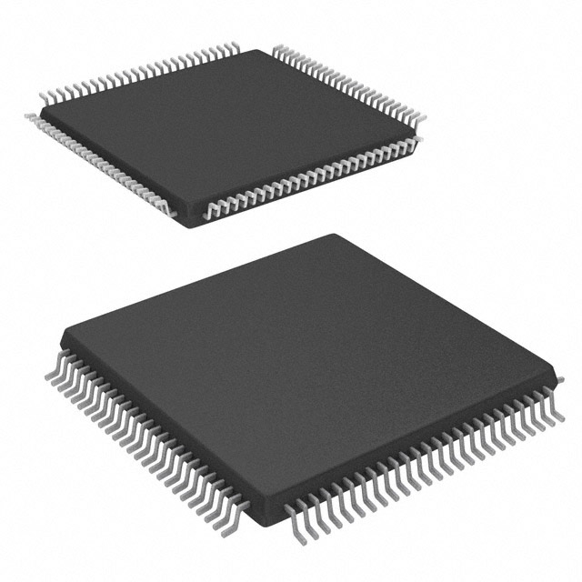
- Part No.:
- CY7C924ADX-AXC
- Manufacturer:
- Infineon Technologies
- Category:
- Drivers, Receivers, Transceivers
- Package:
- 100-LQFP
- Datasheet:
-
 CY7C924ADX-AXC.pdf
- Description:
- IC TRANSCEIVER FULL 100TQFP
- Quantity:
- Payment:

- Shipping:

Inventory:3,431
Please send an inquiry. Send us your inquiry, and we will respond immediately.
Product details
Overview
CY7C924ADX from Cypress Semiconductor Corporation is a second-generation HOTLink® transceiver IC for high-speed point-to-point serial data transport over fiber or copper at 50–200 MBaud. It integrates dual PECL-compatible differential I/O, embedded 8B/10B encoder/decoder, synchronous FIFOs (256×10/8), and on-chip PLL clock recovery - enabling Fibre Channel and ESCON®-compliant links in backplane interconnects and video transmission systems.
For engineers reviewing the CY7C924ADX datasheet, CY7C924ADX pinout, CY7C924ADX application, or CY7C924ADX equivalent, key selection considerations include its configurable 8/10-bit parallel interface, UTOPIA-compatible host bus support, built-in BIST for link validation, and daisy-chain/ring topology capability - all in a 100-pin TQFP package with single +5.0V supply operation.
Technical Context
The CY7C924ADX implements a full-duplex transceiver architecture with independent transmit and receive paths, each featuring a programmable-width parallel interface (8 or 10 bits), selectable raw or 8B/10B encoded mode, and integrated FIFO buffering. Its transmit section includes a 256-character FIFO, 8B/10B encoder, serializer, and dual PECL drivers operating at 10× or 12× character rate.
The receive path uses fully integrated PLL-based clock/data recovery, deserializer, framer, 8B/10B decoder, error detection, and a matching 256-character FIFO. It supports asynchronous TTL parallel I/O, loopback testing, link quality indication, and bypassable encoding/FIFO for reference-locked or externally encoded data transport.
Key Specifications
| Parameter | Value and Actual Design Meaning |
|---|---|
| Serial Rate | 50–200 MBaud - supports scalable link bandwidth without changing physical layer components. |
| Parallel Interface Width | 8 or 10 bits - enables compatibility with UTOPIA Level 1/2 and custom packet-oriented host buses. |
| FIFO Depth | 256 characters × 8/10 bits - absorbs timing skew between host and serial domains; bypassable for deterministic latency. |
| Encoding Scheme | Embedded 8B/10B - ensures DC balance, bounded run length, and control character framing for Fibre Channel/ESCON compliance. |
| Supply Voltage | +5.0 V ±10% - single-rail operation simplifies power design versus multi-voltage transceivers. |
| Differential I/O | Dual PECL-compatible inputs/outputs - directly interfaces with industry-standard fiber modules and balanced copper drivers. |
| Built-in Test | On-chip BIST pattern generator/checker - validates serial path integrity at full speed without external test equipment. |
Pinout & Package
Package: 100-pin Thin Quad Flat Package (TQFP), 0.35 µm CMOS technology, Pb-free option available.
| Pin/Terminal | Circuit Role | Design Meaning |
|---|---|---|
| TXDATA[7:0] | Parallel transmit data input | Configurable 8-bit bus accepting host data; functions as LSBs when encoder bypassed in 10/12-bit raw mode. |
| RXDATA[7:0] | Parallel receive data output | Delivers decoded 8-bit characters to host; retains alignment and framing integrity post-deserialization. |
| TXCLK / RXCLK | Transmit/receive FIFO clock input | Synchronizes parallel interface timing; supports both UTOPIA and cascade timing modes via EXTFIFO control. |
| INA+/INA−, INB+/INB− | Differential serial receive inputs | Accept PECL-level signals from two independent serial lanes; enable ring/daisy-chain topology support. |
| OUTA+/OUTA−, OUTB+/OUTB− | Differential serial transmit outputs | Drive PECL-compatible fiber or copper media; support dual-lane 200 MBaud operation with 10×/12× serialization. |
| TXFULL*/TXHALF*/TXEMPTY* | FIFO status flags | Real-time hardware handshaking signals indicating buffer occupancy - critical for flow control without software polling. |
| FIFOBYP*, ENCBYP*, BYTE8/10* | Configuration control inputs | Enable/disable FIFO buffering, 8B/10B encoding, and parallel width selection - configure for raw transport or protocol-compliant mode. |
Key Features
| Feature | Design Value |
|---|---|
| Integrated PLL clock recovery | Eliminates need for external PLL components while maintaining jitter tolerance < 0.3 UI for 200 MBaud operation. |
| Dual differential PECL I/O | Supports redundant or load-balanced serial links; compatible with standard SFF-8431 and FC-AL optical modules. |
| Configurable FIFO depth & bypass | 256×10/8 FIFO provides elasticity for bursty traffic; bypass mode achieves sub-20 ns fixed latency for real-time applications. |
| UTOPIA Level 1/2 emulation | Enables drop-in replacement in ATM and packet-switching systems without modifying host controller logic. |
| Built-in Self-Test (BIST) | Validates full transmit/receive path at operational speed using PRBS7 patterns - reduces system-level debug time. |
Applications
| Backplane Interconnect | Video Transport System |
|---|---|
|
Use Scenario: High-bandwidth communication between line cards in telecom chassis using balanced copper traces. IC Role / Device Role / Timing Role: Serial link transceiver converting parallel UTOPIA bus data into synchronized 200 MBaud differential streams. Use Value: Replaces wide parallel buses with two differential pairs, reducing EMI, crosstalk, and connector pin count while maintaining deterministic latency. |
Use Scenario: Uncompressed digital video streaming from camera head to processing unit over coaxial cable. IC Role / Device Role / Timing Role: Point-to-point serializer/deserializer handling 10-bit pixel data with embedded sync and error signaling. Use Value: Enables 200 MBaud transport of 4:2:2 YUV video with built-in Link Quality Indicator for real-time signal integrity monitoring. |
| Fibre Channel Node Interface | ESCON-Compatible Storage Link |
|
Use Scenario: Host bus adapter connecting server to Fibre Channel fabric using short-reach optical modules. IC Role / Device Role / Timing Role: Protocol-transparent transceiver implementing 8B/10B encoding/decoding per FC-PH spec. Use Value: Achieves Fibre Channel Class 1 compliance without external encoder; supports 106.25 MBaud (1×) and 212.5 MBaud (2×) rates via SPDSEL configuration. |
Use Scenario: Mainframe-to-storage subsystem link using legacy ESCON infrastructure with copper or fiber. IC Role / Device Role / Timing Role: ESCON-compliant serial transceiver with domain addressing and daisy-chain topology support. Use Value: Maintains ESCON timing and framing while adding modern diagnostics (BIST, LQI) and flexible FIFO buffering for legacy migration. |
Equivalent & Alternatives
The following parts are listed as comparable options for similar high-speed serial transceiver applications.
| Alternative Part | Technical Difference | Application Difference | Selection Advice |
|---|---|---|---|
| TI SN65LVDS32 | LVDS-based, 400 Mbps max, no embedded 8B/10B or FIFO - requires external encoding logic. | Limited to simpler point-to-point links without protocol framing or link-layer diagnostics. | Select when cost-sensitive, low-jitter LVDS links suffice and host handles encoding/flow control. |
| Maxim MAX3283 | PECL-compatible, 250 Mbps, no integrated FIFO or BIST - minimal feature set focused on physical layer only. | Suitable for basic serial extension but lacks topology flexibility and self-test capability. | Choose for space-constrained designs needing only differential driver/receiver functionality. |
Compared with SN65LVDS32 and MAX3283, the CY7C924ADX delivers higher integration (FIFO, encoder, PLL, BIST), broader protocol support (Fibre Channel/ESCON), and topology versatility (ring/daisy-chain), making it optimal for complex embedded serial infrastructure where reliability and diagnostics matter.
Availability
CY7C924ADX is available at Aetrix Electronics and suitable for backplane interconnects, video transport systems, Fibre Channel node interfaces, and ESCON-compatible storage links requiring stable component supply across extended product lifecycles.
Supply support for CY7C924ADX includes scheduled delivery planning, volume procurement assistance, BOM continuity management, traceable sourcing, and lifecycle availability coordination for OEM customers, industrial embedded developers, connected-device designers, and electronics production programs.
Manufacturer
Cypress Semiconductor (now part of Infineon Technologies) is a fabless semiconductor company specializing in high-performance mixed-signal and programmable solutions for connectivity, memory, and embedded control.
The CY7C924ADX belongs to Cypress's HOTLink® transceiver family, designed specifically to replace parallel buses with robust, low-latency, protocol-aware serial links in telecom, storage, and video infrastructure.
FAQ
Does CY7C924ADX support both 8-bit and 10-bit parallel interfaces simultaneously?
No. The parallel interface width is configured at power-up via the BYTE8/10* pin: LOW selects 10-bit mode (TXDATA[9:0], RXDATA[9:0]), HIGH selects 8-bit mode (TXDATA[7:0], RXDATA[7:0]). This setting determines FIFO depth interpretation and encoding behavior, and cannot be changed dynamically during operation.
Can the CY7C924ADX operate without an external crystal or reference clock?
Yes. The device uses internal PLLs for clock multiplication and recovery, requiring only a single REFCLK input (typically derived from the host system clock). No external crystal or oscillator is needed - REFCLK may be sourced from the host's clock tree or a dedicated oscillator, with frequency selected per SPDSEL and RANGESEL settings.
What is the function of the AM* pin in CY7C924ADX?
AM* (Address Match Enable) controls the output enable state of TXFULL*, TXHALF*, and TXEMPTY* status flags. When AM* is asserted LOW, these outputs are placed in high-impedance state; when AM* is HIGH, they drive active logic levels. This allows multiple CY7C924ADX devices to share status lines on a common bus without contention.
How does Built-In Self-Test (BIST) validate link integrity?
BIST generates and checks PRBS7 patterns end-to-end: internally injected into the transmit path, sent across the serial link, received, decoded, and compared against expected sequence. It verifies both transmitter and receiver functionality - including serialization/deserialization, clock recovery, and 8B/10B coding - at full operational speed without external test gear.
CY7C924ADX-AXC Specifications
- Product attributes
- Attribute value
- Manufacturer:
- Infineon Technologies
- Series:
- HOTlink™
- Package/Case:
- 100-LQFP
- Packaging:
- Tray
- Product Status:
- Obsolete
- Type:
- Transceiver
- Protocol:
- Fibre Channel
- Number of Drivers/Receivers:
- -
- Duplex:
- Full
- Receiver Hysteresis:
- -
- Data Rate:
- -
- Voltage - Supply:
- 4.5V ~ 5.5V
- Operating Temperature:
- 0°C ~ 70°C
- Grade:
- -
- Qualification:
- -
- Mounting Type:
- Surface Mount
- Supplier Device Package:
- 100-TQFP (14x14)
CY7C924ADX-AXC FAQ
1.How can I place an order for CY7C924ADX-AXC through Aetrix?
Please submit a Request for Quotation (RFQ) for CY7C924ADX-AXC on Aetrix. Our sales agent will provide a competitive quotation and guide you through the order confirmation once you accept the terms.
2.Are the price and stock information for CY7C924ADX-AXC reliable?
The price and inventory of CY7C924ADX-AXC are updated periodically and may fluctuate due to market conditions. Stock and pricing data are typically refreshed every 24 hours. Quotation validity for CY7C924ADX-AXC is usually 5 days.
3.What payment methods are accepted for CY7C924ADX-AXC?
We accept Wire Transfer, PayPal, Credit Card, Western Union, MoneyGram, and Escrow for CY7C924ADX-AXC transactions.
Note: Certain payment methods may incur a processing fee.
4.How is shipping managed for CY7C924ADX-AXC?
CY7C924ADX-AXC orders can be shipped via leading logistics carriers, including DHL, UPS, FedEx, TNT, or Registered Mail.
Once your CY7C924ADX-AXC order is processed, you will receive an email with the shipment details and tracking number.
Note: Tracking information may take up to 24 hours to appear. Express delivery typically takes 3–5 business days.
5.How can I obtain technical support or documentation for CY7C924ADX-AXC?
For technical support, including CY7C924ADX-AXC datasheets, pinout diagrams, or application guidance, please contact our engineering support team. They can provide detailed documentation and assistance for your CY7C924ADX-AXC requirements.
6.How does Aetrix verify that CY7C924ADX-AXC is sourced from the original manufacturer or authorized distributors?
All CY7C924ADX-AXC products on Aetrix are procured from qualified distributors and authorized channels. Our dedicated quality assurance team conducts strict verification, including traceability checks and, if necessary, third-party testing. This ensures that CY7C924ADX-AXC meets industry standards.
7.What is the process for return or replacement of CY7C924ADX-AXC?
All CY7C924ADX-AXC units undergo pre-shipment inspection (PSI). If there is an issue with CY7C924ADX-AXC, returns or replacements are accepted under the following conditions:
1.Quantity discrepancies, incorrect items, or visible external defects (such as breakage or corrosion), acknowledged by Aetrix.
2.The issue is reported within 90 days of delivery.
3.The CY7C924ADX-AXC part is unused and in its original packaging.
Return procedure for CY7C924ADX-AXC:
1.Submit a request within 90 days.
2.Obtain a Return Material Authorization (RMA) from Aetrix.
CY7C924ADX-AXC Tags

-
ATA6561-GAQW-N
Microchip Technology
-
ATA6561-GBQW-N
Microchip Technology

-
AM26LS32ACDR
Texas Instruments

-
SP485CN-L/TR
MaxLinear, Inc.
-
SP485EN-L/TR
MaxLinear, Inc.
-
SP485EEN-L/TR
MaxLinear, Inc.
-
SP485ECN-L/TR
MaxLinear, Inc.
-
THVD1400DR
Texas Instruments
-
AM26C31IDR
Texas Instruments

-
TLIN1021ADRQ1
Texas Instruments
-
MAX232IDR
Texas Instruments
-
AM26C32IDR
Texas Instruments
Tech Hub

LDO regulator guide covering low dropout voltage, power dissipation, thermal design, PSRR, output noise, capacitor stability, adjustable LDO circuits, LDO vs buck converter and datasheet selection chec…

Conditional Access Module guide covering CAM meaning, CI/CI+ interface, smart card authorization, DVB security workflow, TV and set-top box compatibility, internal electronics, ESD protection, connecto…

Guide to electronic component obsolescence covering EOL risk, PCN/PDN notices, last-time buy planning, replacement options, form-fit-function validation, counterfeit risk and BOM lifecycle management.

18650 battery guide covering lithium-ion cell basics, 3.6V/3.7V voltage, 4.2V charging, mAh and Wh capacity, protected cells, chargers, BMS, series-parallel packs, holders, welding and sourcing checks.…

Hall effect sensor guide covering working principle, linear and digital sensors, Arduino circuits, current sensing, speed detection, automotive applications, A3144 examples, signal filtering and datash…

Product Change Notification guide for electronic components, covering PCN meaning, PCN vs PDN/EOL, common change types, risk levels, form-fit-function review, engineering validation, BOM control, LTB/L…

A practical guide to blend door actuators, covering HVAC function, symptoms, location, AC and heater issues, reset and calibration, replacement cost, electrical diagnosis, compatibility checks, and rep…

Engineering guide to Raspberry Pi alternatives, covering chip-level differences, Orange Pi, ROCK, Jetson, Banana Pi, NanoPi, Compute Module, Pico, GPIO, camera, HAT compatibility, and replacement risks…

Engineering guide to dynamic load response testing for high-current buck converters, covering load step setup, slew rate, Vcore undershoot, overshoot, recovery time, probe location, output capacitors a…

Engineering guide to output capacitor selection for ASIC Vcore rails, covering bulk capacitors, polymer capacitors, MLCC decoupling, DC bias, ESR, ESL, placement, transient response and substitution ri…


