
 My Inquiry
 My Account


Infineon Technologies CYUSB2014-BZXI
- Part No.:
- CYUSB2014-BZXI
- Manufacturer:
- Infineon Technologies
- Category:
- Application Specific Microcontrollers
- Package:
- 121-TFBGA
- Datasheet:
-
 CYUSB2014-BZXI.pdf
- Description:
- IC EZ-USB BRIDGE FX3 3.0 121BGA
- Quantity:
- Payment:

- Shipping:

Inventory:877
Please send an inquiry. Send us your inquiry, and we will respond immediately.
Product details
Overview
CYUSB2014-BZXI from Infineon is a USB 3.2 Gen 1 and USB 2.0 peripheral controller featuring an ARM926EJ-S core running at 200 MHz, 256 KB embedded SRAM, and a programmable 100-MHz GPIF II interface supporting 8-/16-/24-/32-bit buses. It integrates USB 3.2 SuperSpeed PHY (5 Gbps), HS-OTG host/peripheral capability, and 32 physical endpoints. Used in high-bandwidth video capture cards and industrial cameras for real-time sensor-to-PC streaming.
For engineers reviewing the CYUSB2014-BZXI datasheet, CYUSB2014-BZXI pinout, CYUSB2014-BZXI application, or CYUSB2014-BZXI equivalent, key selection criteria include GPIF II timing compliance, USB 3.2 Gen 1 enumeration stability, ARM926EJ-S firmware debug access via JTAG, and 1.2-V core / 1.8–3.3-V I/O voltage domain separation.
Technical Context
The CYUSB2014-BZXI implements a dual-mode USB controller with full USB 3.2 Gen 1 (5 Gbps) and backward-compatible USB 2.0 (480 Mbps) transceivers. Its ARM926EJ-S CPU executes firmware directly from on-chip SRAM and supports ThreadX RTOS integration via the EZ-USB FX3 SDK.
GPIF II operates as a synchronous state-machine-driven parallel interface with configurable clocking (up to 100 MHz), programmable bus width, and up to 16 control signals - enabling direct connection to FPGAs, image sensors, and memory-mapped peripherals without external glue logic.
Key Specifications
| Parameter | Value and Actual Design Meaning |
|---|---|
| USB Compliance | USB 3.2 Gen 1 (5 Gbps) + USB 2.0 High-Speed (480 Mbps); TID #340800007 certified |
| CPU Core | ARM926EJ-S @ 200 MHz; enables real-time firmware execution with JTAG debug support |
| Embedded Memory | 256 KB SRAM; sufficient for UVC-compliant video streaming firmware and descriptor handling |
| GPIF II Bus Width | Configurable 8/16/24/32-bit; matches common image sensor and FPGA data bus widths |
| Power Domains | Independent 1.2-V core + 1.8–3.3-V I/O; allows interfacing with mixed-voltage peripherals |
| OTG Support | HS-OTG host/peripheral per OTG Supplement v2.0; enables dual-role operation in portable devices |
| Crystal Input | 19.2 MHz fundamental-mode crystal; provides stable reference for USB packet timing and PLL lock |
Pinout & Package
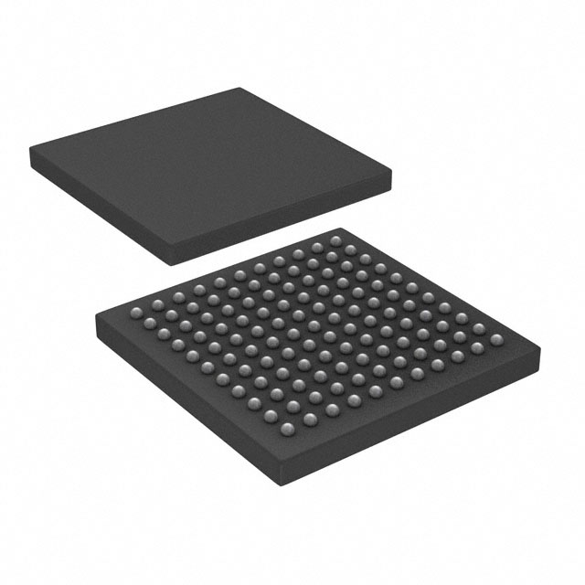
Package: 121-ball, 10 mm × 10 mm, 0.8-mm pitch Pb-free BGA (package code BZXI).
| Pin/Terminal | Circuit Role | Design Meaning |
|---|---|---|
| VBATT | Battery power supply input | Enables ultra-low-power mode (<20 µA) when core is powered down but battery remains active |
| VDD_CORE | Core logic supply | 1.2-V regulated input; powers ARM926EJ-S CPU and internal SRAM |
| VDD_IO | I/O supply | 1.8–3.3-V selectable; sets voltage level for GPIF II, UART, SPI, and I2C pins |
| XTAL_IN / XTAL_OUT | Clock oscillator terminals | Accepts 19.2-MHz fundamental crystal; drives internal PLL for USB 3.2 timing accuracy |
| USB_DP / USB_DM | SuperSpeed differential pair | 5-Gbps USB 3.2 Gen 1 signaling; requires controlled 90-Ω differential impedance routing |
| GPIF_AD[0:31] | Data/address bus | Configurable as 8/16/24/32-bit parallel interface; timing-synchronized to PCLK |
| JTAG_TCK / TMS / TDI / TDO | Debug interface | Supports full boundary-scan and firmware debug via standard ARM JTAG chain |
Key Features
| Feature | Design Value |
|---|---|
| Programmable GPIF II | Graphically configurable state machine (via GPIF II Designer) eliminates need for external FIFO or bridge ICs in sensor/FPGA interfaces |
| USB ReNumeration | Runtime device class switching (e.g., UVC → MSC) without host driver reload - critical for multi-function peripherals |
| Slave FIFO Mode | Hardware-accelerated data transfer between USB and external logic; achieves >350 MB/s sustained throughput in synchronous 32-bit mode |
| Boot Flexibility | Supports boot from SPI flash, I2C EEPROM, or USB host download - simplifies field firmware updates and factory programming |
| ESD Protection | ±8 kV HBM on USB pins; meets IEC 61000-4-2 Level 3 for industrial camera and test equipment deployment |
Applications
| Digital Video Capture Card | Industrial Camera Interface |
|---|---|
Use Scenario: Real-time HDMI/SDI-to-USB3 conversion for PC-based vision analysis. IC Role / Device Role / Timing Role: USB peripheral controller with GPIF II acting as synchronous slave FIFO to FPGA video pipeline. Use Value: Eliminates external USB bridge IC; enables sub-100 µs frame latency using hardware handshaking (SLRD/SLWR) and 100-MHz PCLK. | Use Scenario: High-resolution CMOS sensor data acquisition in factory automation systems. IC Role / Device Role / Timing Role: Host-side USB endpoint managing burst transfers from sensor over parallel GPIF II bus. Use Value: Sustained 320 MB/s throughput (32-bit @ 100 MHz) meets 4K@60fps raw Bayer streaming requirements. |
| Medical Imaging Device | Test & Measurement Equipment |
Use Scenario: Ultrasound probe data streaming to diagnostic workstation via USB 3.2. IC Role / Device Role / Timing Role: USB 3.2 Gen 1 peripheral with renumerated UVC + custom class descriptors for proprietary imaging protocols. Use Value: Dual-class enumeration preserves Windows UVC driver compatibility while enabling vendor-specific control channel via CDC ACM interface. | Use Scenario: High-speed logic analyzer data offload from FPGA acquisition buffer to host PC. IC Role / Device Role / Timing Role: USB device controller with asynchronous Slave FIFO mode for variable-length trigger-captured samples. Use Value: Hardware FIFO depth (up to 16 KB) absorbs jitter between FPGA sampling clock and USB packet boundaries. |
Equivalent & Alternatives
The following parts are listed as comparable options for similar USB 3.2 peripheral controller applications.
| Alternative Part | Technical Difference | Application Difference | Selection Advice |
|---|---|---|---|
| CYUSB3014-BZXI | 512 KB SRAM, same package and pinout | Higher memory headroom for complex UVC + audio + HID composite devices | Select when firmware exceeds 256 KB or requires dual simultaneous streaming pipelines |
| CX3-EBZ | MIPI CSI-2 receiver integrated; no GPIF II; fixed 2-lane CSI-2 + USB 3.0 | Optimized for direct CMOS image sensor connection only - no general-purpose parallel interface | Select only for MIPI-based camera modules where sensor output is CSI-2, not parallel |
Compared with CYUSB3014-BZXI, this part trades SRAM capacity for cost and footprint; compared with CX3-EBZ, it offers full GPIF II flexibility at the expense of dedicated MIPI support - making it optimal for non-MIPI, high-customization USB peripheral designs.
Availability
CYUSB2014-BZXI is available at Aetrix Electronics and suitable for digital video capture cards, industrial camera interfaces, and medical imaging devices requiring stable component supply across long-life production cycles.
Supply support for CYUSB2014-BZXI includes scheduled delivery planning, volume procurement assistance, BOM continuity management, traceable sourcing, and lifecycle availability coordination for OEM customers, industrial embedded developers, connected-device designers, and electronics production programs.
Manufacturer
Infineon Technologies is a German semiconductor manufacturer specializing in power management, automotive MCUs, and high-speed connectivity solutions, with global R&D and manufacturing infrastructure.
CYUSB2014-BZXI belongs to the EZ-USB FX3 family - designed specifically for embedded USB 3.2 peripheral applications requiring programmable parallel interfaces, real-time firmware control, and industrial-grade reliability.
FAQ
What boot sources does CYUSB2014-BZXI support?
CYUSB2014-BZXI supports boot from internal ROM (for recovery), SPI flash (primary production method), I2C EEPROM, and USB host download via vendor command. Boot mode is selected by GPIO strap pins at power-up, and the EZ-USB FX3 SDK provides tools to generate signed firmware images for secure SPI boot.
Does CYUSB2014-BZXI require an external USB PHY?
No. CYUSB2014-BZXI integrates a fully compliant USB 3.2 Gen 1 (5 Gbps) SuperSpeed PHY and USB 2.0 High-Speed PHY. Only passive termination (22-Ω series resistors on USB_DP/DM, 45-Ω AC-coupling caps) and proper PCB layout per Infineon's AN70707 are required - no external PHY chip needed.
Can GPIF II operate synchronously with an external clock source?
Yes. GPIF II can be configured to use an external clock (PCLK_EXT) instead of the internal 100-MHz clock. This allows synchronization to an external video pixel clock or FPGA system clock, ensuring deterministic phase alignment for time-critical sensor data capture without FIFO resynchronization overhead.
Is JTAG debugging supported in all power modes?
JTAG is fully functional in active and sleep modes but disabled in deep power-down (core power-off) mode where VBATT is present. When VBATT is removed, JTAG is inactive until VDD_CORE is restored. Debug access remains available during low-power suspend states where CPU clocks are gated but SRAM retention is maintained.
CYUSB2014-BZXI Specifications
- Product attributes
- Attribute value
- Manufacturer:
- Infineon Technologies
- Series:
- EZ-USB FX3™
- Package/Case:
- 121-TFBGA
- Packaging:
- Tray
- Product Status:
- Active
- Programmable:
- Not Verified
- Applications:
- SuperSpeed USB Peripheral Controller
- Core Processor:
- ARM9®
- Program Memory Type:
- External Program Memory
- Controller Series:
- CYUSB
- RAM Size:
- 512K x 8
- Interface:
- I2C, I2S, MMC/SD, SPI, UART, USB
- Number of I/O:
- 59
- Voltage - Supply:
- 1.15V ~ 1.25V
- Operating Temperature:
- -40°C ~ 85°C
- Grade:
- -
- Qualification:
- -
- Mounting Type:
- Surface Mount
- Supplier Device Package:
- 121-FBGA (10x10)
CYUSB2014-BZXI FAQ
1.How can I place an order for CYUSB2014-BZXI through Aetrix?
Please submit a Request for Quotation (RFQ) for CYUSB2014-BZXI on Aetrix. Our sales agent will provide a competitive quotation and guide you through the order confirmation once you accept the terms.
2.Are the price and stock information for CYUSB2014-BZXI reliable?
The price and inventory of CYUSB2014-BZXI are updated periodically and may fluctuate due to market conditions. Stock and pricing data are typically refreshed every 24 hours. Quotation validity for CYUSB2014-BZXI is usually 5 days.
3.What payment methods are accepted for CYUSB2014-BZXI?
We accept Wire Transfer, PayPal, Credit Card, Western Union, MoneyGram, and Escrow for CYUSB2014-BZXI transactions.
Note: Certain payment methods may incur a processing fee.
4.How is shipping managed for CYUSB2014-BZXI?
CYUSB2014-BZXI orders can be shipped via leading logistics carriers, including DHL, UPS, FedEx, TNT, or Registered Mail.
Once your CYUSB2014-BZXI order is processed, you will receive an email with the shipment details and tracking number.
Note: Tracking information may take up to 24 hours to appear. Express delivery typically takes 3–5 business days.
5.How can I obtain technical support or documentation for CYUSB2014-BZXI?
For technical support, including CYUSB2014-BZXI datasheets, pinout diagrams, or application guidance, please contact our engineering support team. They can provide detailed documentation and assistance for your CYUSB2014-BZXI requirements.
6.How does Aetrix verify that CYUSB2014-BZXI is sourced from the original manufacturer or authorized distributors?
All CYUSB2014-BZXI products on Aetrix are procured from qualified distributors and authorized channels. Our dedicated quality assurance team conducts strict verification, including traceability checks and, if necessary, third-party testing. This ensures that CYUSB2014-BZXI meets industry standards.
7.What is the process for return or replacement of CYUSB2014-BZXI?
All CYUSB2014-BZXI units undergo pre-shipment inspection (PSI). If there is an issue with CYUSB2014-BZXI, returns or replacements are accepted under the following conditions:
1.Quantity discrepancies, incorrect items, or visible external defects (such as breakage or corrosion), acknowledged by Aetrix.
2.The issue is reported within 90 days of delivery.
3.The CYUSB2014-BZXI part is unused and in its original packaging.
Return procedure for CYUSB2014-BZXI:
1.Submit a request within 90 days.
2.Obtain a Return Material Authorization (RMA) from Aetrix.
CYUSB2014-BZXI Tags

-
CYPD3175-24LQXQ
Infineon Technologies

-
SLB9672VU20FW1523XTMA1
Infineon Technologies

-
SLB9670VQ20FW785XTMA1
Infineon Technologies
-
SLB9672XU20FW1523XTMA1
Infineon Technologies
-
SLB9673XU20FW2613XTMA1
Infineon Technologies

-
CYPD3125-40LQXIT
Infineon Technologies

-
AT97SC3204-U2A1A-20
Microchip Technology
-
AT97SC3204-U2A1A-10
Microchip Technology
-
SLM9670AQ20FW1311XTMA1
Infineon Technologies
-
SLB9672XU20FW1613XTMA1
Infineon Technologies
-
SLB9672AU20FW1613XTMA1
Infineon Technologies
-
SLB9673AU20FW2613XTMA1
Infineon Technologies
Tech Hub

18650 battery guide covering lithium-ion cell basics, 3.6V/3.7V voltage, 4.2V charging, mAh and Wh capacity, protected cells, chargers, BMS, series-parallel packs, holders, welding and sourcing checks.…

Hall effect sensor guide covering working principle, linear and digital sensors, Arduino circuits, current sensing, speed detection, automotive applications, A3144 examples, signal filtering and datash…

Product Change Notification guide for electronic components, covering PCN meaning, PCN vs PDN/EOL, common change types, risk levels, form-fit-function review, engineering validation, BOM control, LTB/L…

A practical guide to blend door actuators, covering HVAC function, symptoms, location, AC and heater issues, reset and calibration, replacement cost, electrical diagnosis, compatibility checks, and rep…

Engineering guide to Raspberry Pi alternatives, covering chip-level differences, Orange Pi, ROCK, Jetson, Banana Pi, NanoPi, Compute Module, Pico, GPIO, camera, HAT compatibility, and replacement risks…

Engineering guide to dynamic load response testing for high-current buck converters, covering load step setup, slew rate, Vcore undershoot, overshoot, recovery time, probe location, output capacitors a…

Engineering guide to output capacitor selection for ASIC Vcore rails, covering bulk capacitors, polymer capacitors, MLCC decoupling, DC bias, ESR, ESL, placement, transient response and substitution ri…

Engineering guide to high-current ASIC Vcore rails, covering 12-phase buck architecture, PMBus control, dynamic load testing, output capacitor networks, smart power stage selection, thermal design and …

Voltage regulator guide covering linear, LDO, 7805, Zener, adjustable, buck, VRM and alternator regulators, with design checks, testing methods, troubleshooting and datasheet-based selection.

Amplifier guide covering voltage, current and power amplification, gain, feedback, amplifier classes, audio and RF applications, op-amp circuits, transimpedance amplifiers, datasheet selection and trou…


