Send an Inquiry

To receive a quote for your project, please fill in the following information, and we’ll get back to you promptly.

Name*
Company*
Email Address*
Phone/WhatsApp
Part Number*
Quantity*
Message
Submit Inventory List

Please fill in the following information, and we’ll get back to you promptly.

Name*
Company*
Email Address*
Phone/WhatsApp
Upload My List
Message

Vishay Siliconix DG184BP

Part No.:
DG184BP
Manufacturer:
Vishay Siliconix
Category:
Analog Switches, Multiplexers, Demultiplexers
Package:
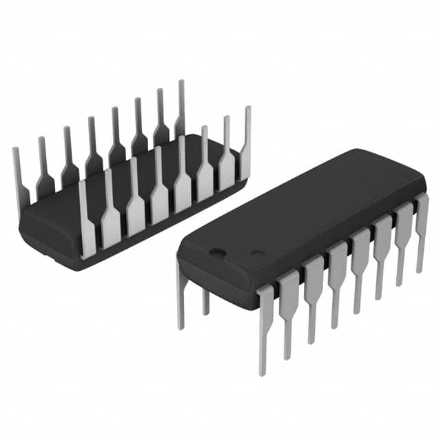
16-DIP (0.300", 7.62mm)
Datasheet:
AetrixDG184BP.pdf
Description:
IC SWITCH DPST-NOX2 50OHM 16DIP
Quantity:
Payment:
Payment
Shipping:
Shipping

Inventory:4,381

Please send an inquiry. Send us your inquiry, and we will respond immediately.

Part Number
Quantity*
Price
Name*
Company
Email*
Comments

Product details

Overview

DG184BP from Vishay Siliconix is a precision dual double-pole, single-throw (DPST) JFET analog switch optimized for high-fidelity audio and video signal routing. It features 30 Ω typical on-resistance (rDS(on)), <2 nA channel-on leakage (ID(on)), 85–180 ns turn-on time, ±15 V dual supply operation, and operates over –25 °C to +85 °C in aerospace-grade 16-pin sidebraze packaging.

For engineers reviewing the DG184BP datasheet, DG184BP pinout, DG184BP application, or DG184BP equivalent, key selection criteria include constant on-resistance across full analog range (–12.5 V to +10 V), break-before-make switching behavior, low crosstalk (>50 dB off-isolation at 1 MHz), and radiation-hardened construction suitable for mission-critical signal path control.

Technical Context

The DG184BP integrates four n-channel JFETs with TTL-compatible bipolar logic drivers to enable bidirectional analog conduction in the on-state and 20 V peak-to-peak blocking capability in the off-state. Its flat rDS(on) profile eliminates large-signal distortion and ensures consistent gain across the analog input range.

Switching is controlled by two independent digital inputs (IN1, IN2), each driving a pair of complementary JFETs per pole. Logic thresholds are fixed at VINH ≥ 2.0 V and VINL ≤ 0.8 V, with dedicated VL (5 V logic supply) and VR (reference ground) pins decoupling logic and analog domains.

Key Specifications

ParameterValue and Actual Design Meaning
Analog Signal Range–12.5 V to +10 V - supports wide dynamic range video and audio signals without clipping
rDS(on)30 Ω max - ensures minimal insertion loss and predictable gain in precision signal paths
ID(on)<2 nA - prevents DC offset drift and signal corruption in sample/hold and high-Z sensor interfaces
Turn-On/Off Time85/95 ns typ - enables fast multiplexing in real-time video routing and data acquisition systems
Off Isolation>50 dB at 1 MHz - suppresses inter-channel crosstalk critical for multi-source video switching
Supply Voltage RangeV+ = +15 V, V– = –15 V - dual-rail support for bipolar analog signal handling
Logic SupplyVL = 5 V - standard TTL-level compatibility without level-shifting circuitry

Pinout & Package

Package: 16-pin sidebraze ceramic hermetic package (MIL-STD-1835 compliant), rated for –25 °C to +85 °C operating temperature.

Pin/TerminalCircuit RoleDesign Meaning
1, 2, 3, 4S1, S2, S3, S4Source terminals for four JFET switches - form two DPST channels (S1/S2 = Ch1, S3/S4 = Ch2)
5, 6, 7, 8D1, D2, D3, D4Drain terminals paired with respective sources - bidirectional current path with matched rDS(on)
9, 10IN1, IN2Digital control inputs - TTL-compatible; activate corresponding DPST channel when high
11V+Positive analog supply - powers JFET channels and sets upper analog signal limit
12V–Negative analog supply - sets lower analog signal limit and bias for JFET operation
13VLLogic supply - powers internal driver circuitry; must be 5 V for guaranteed switching performance
14VRReference ground - dedicated return for logic domain; isolates noise from analog ground
15, 16NCNo connect - internally unused; must remain unconnected per datasheet

Key Features

FeatureDesign Value
Constant on-resistance over full analog rangeEnables distortion-free switching of large-amplitude signals without gain variation or harmonic generation
Break-before-make switchingPrevents momentary shorting between channels during state transitions - critical for fault-tolerant routing
Radiation hardnessQualified per MIL-PRF-38535 Class B - suitable for space and high-reliability defense avionics
Low charge injection (<1 pC)Minimizes voltage spikes at output edges - preserves integrity in sample-and-hold and precision ADC front-ends
High channel isolation (>50 dB)Reduces interference between active and inactive signal paths - essential for multi-channel video matrix switching

Applications

Audio SwitchingVideo Routing

Use Scenario: Selecting between multiple microphone or line-level inputs in a studio-grade mixing console.

IC Role / Device Role / Timing Role: Dual DPST analog switch providing isolated, low-distortion signal path selection under microcontroller control.

Use Value: Flat 30 Ω rDS(on) ensures consistent frequency response across all inputs; sub-2 nA leakage prevents DC bias shift in high-gain preamp stages.

Use Scenario: Routing composite or component video signals among cameras, recorders, and displays in broadcast equipment.

IC Role / Device Role / Timing Role: Precision analog switch enabling fast, glitch-free source selection with minimal crosstalk between video channels.

Use Value: >50 dB off-isolation at 1 MHz suppresses ghosting and color bleed; 85 ns turn-on supports real-time switching without visible artifacts.

Sample/Hold CircuitsAerospace Signal Conditioning

Use Scenario: Capturing precise analog sensor outputs (e.g., temperature, pressure) in data acquisition systems.

IC Role / Device Role / Timing Role: Low-leakage, low-charge-injection switch controlling hold capacitor connection to signal source.

Use Value: <2 nA ID(on) prevents hold capacitor discharge drift; minimal charge injection avoids sampling pedestal error.

Use Scenario: Multiplexing telemetry signals from redundant sensors in satellite payload subsystems.

IC Role / Device Role / Timing Role: Radiation-hardened DPST switch performing fault-protected signal path selection in harsh orbital environments.

Use Value: MIL-PRF-38535 qualification ensures operational reliability; break-before-make action prevents bus contention during reconfiguration.

Equivalent & Alternatives

The following parts are listed as comparable options for similar dual DPST analog switch applications.

Alternative PartTechnical DifferenceApplication DifferenceSelection Advice
DG183BPLower rDS(on) (10 Ω max), higher current rating (200 mA vs. 30 mA), same package and pinoutBetter suited for high-current audio line driving; less ideal where ultra-low leakage is primary requirementSelect DG183BP only if on-resistance and current drive outweigh leakage and power trade-offs
DG185BPHigher rDS(on) (75 Ω max), extended analog range (–15 V to +10 V), same logic interface and packagePreferred for wider-voltage industrial sensors; reduced bandwidth due to higher capacitanceChoose DG185BP when signal swing exceeds –12.5 V but speed and leakage tolerance allow higher rDS(on)

Compared with DG184BP, DG183BP delivers lower on-resistance at the cost of higher leakage and power dissipation, while DG185BP extends voltage range but sacrifices switching speed and isolation - making DG184BP the balanced choice for high-fidelity, medium-voltage video/audio routing where leakage, speed, and flat resistance are jointly critical.

Availability

DG184BP is available at Aetrix Electronics and suitable for aerospace telemetry, broadcast video routing, and precision test instrumentation requiring stable component supply, long-term obsolescence management, and traceable military-grade sourcing.

Supply support for DG184BP includes scheduled delivery planning, volume procurement assistance, BOM continuity management, traceable sourcing, and lifecycle availability coordination for OEM customers, industrial embedded developers, connected-device designers, and electronics production programs.

Manufacturer

Vishay Siliconix is a global semiconductor manufacturer specializing in discrete semiconductors, analog switches, and high-reliability passive components.

The DG183/184/185 family was designed specifically for radiation-tolerant, high-precision analog signal routing in aerospace, defense, and broadcast systems where constant on-resistance, low leakage, and break-before-make safety are mandatory.

FAQ

What is the maximum analog signal voltage range supported by the DG184BP?

The DG184BP supports an analog signal range of –12.5 V to +10 V when operated with V+ = +15 V and V– = –15 V. This range is guaranteed by design and enables accurate switching of wide-dynamic-range video and audio signals without clipping or distortion. The device maintains constant on-resistance across this entire span, ensuring linear signal transfer.

Does the DG184BP require external level-shifting for TTL-compatible control inputs?

No, the DG184BP does not require external level-shifting. Its digital inputs (IN1 and IN2) are TTL-compatible with guaranteed recognition of logic high at VINH ≥ 2.0 V and logic low at VINL ≤ 0.8 V. The dedicated VL pin accepts a 5 V supply to power the internal driver, ensuring robust switching performance directly from standard microcontroller or FPGA GPIO outputs.

How does the DG184BP achieve break-before-make switching behavior?

The DG184BP achieves break-before-make switching through internal timing control in its bipolar driver circuitry, which ensures that one channel fully turns off before the other activates. This prevents momentary shorting between signal paths - a critical safety feature in fault-sensitive applications like aerospace telemetry multiplexing. The behavior is inherent to the IC's architecture and requires no external timing components.

What is the significance of the VR pin on the DG184BP?

The VR pin on the DG184BP serves as the dedicated reference ground for the logic domain, electrically isolating it from the analog ground (V–) and power grounds. This separation minimizes noise coupling from digital switching transients into sensitive analog signal paths, improving signal integrity in high-precision applications such as sample-and-hold circuits and broadcast video routing where crosstalk must be strictly controlled.

Is the DG184BP suitable for spaceflight applications?

Yes, the DG184BP is suitable for spaceflight applications. It is manufactured to MIL-PRF-38535 Class B standards, qualified for radiation hardness, and packaged in a hermetic 16-pin sidebraze ceramic case. Its guaranteed performance over –25 °C to +85 °C, low leakage (<2 nA), and break-before-make switching make it appropriate for satellite telemetry, payload signal conditioning, and onboard avionics where reliability under radiation exposure is mandatory.

DG184BP Specifications

Product attributes
Attribute value
Manufacturer:
Vishay Siliconix
Series:
-
Packaging:
Tube
Product Status:
Obsolete
Switch Circuit:
DPST - NO
Multiplexer/Demultiplexer Circuit:
2:1
Number of Circuits:
2
On-State Resistance (Max):
50Ohm
Channel-to-Channel Matching (ΔRon):
-
Voltage - Supply, Single (V+):
-
Voltage - Supply, Dual (V±):
±15V
Switch Time (Ton, Toff) (Max):
180ns, 150ns
-3db Bandwidth:
-
Charge Injection:
-
Channel Capacitance (CS(off), CD(off)):
9pF, 6pF
Current - Leakage (IS(off)) (Max):
5nA
Crosstalk:
-
Operating Temperature:
-25°C ~ 85°C (TA)
Grade:
-
Qualification:
-
Mounting Type:
Through Hole
Supplier Device Package:
16-DIP

DG184BP FAQ

1.How can I place an order for DG184BP through Aetrix?

Please submit a Request for Quotation (RFQ) for DG184BP on Aetrix. Our sales agent will provide a competitive quotation and guide you through the order confirmation once you accept the terms.

2.Are the price and stock information for DG184BP reliable?

The price and inventory of DG184BP are updated periodically and may fluctuate due to market conditions. Stock and pricing data are typically refreshed every 24 hours. Quotation validity for DG184BP is usually 5 days.

3.What payment methods are accepted for DG184BP?

We accept Wire Transfer, PayPal, Credit Card, Western Union, MoneyGram, and Escrow for DG184BP transactions.

Note: Certain payment methods may incur a processing fee.

4.How is shipping managed for DG184BP?

DG184BP orders can be shipped via leading logistics carriers, including DHL, UPS, FedEx, TNT, or Registered Mail.

Once your DG184BP order is processed, you will receive an email with the shipment details and tracking number.

Note: Tracking information may take up to 24 hours to appear. Express delivery typically takes 3–5 business days.

5.How can I obtain technical support or documentation for DG184BP?

For technical support, including DG184BP datasheets, pinout diagrams, or application guidance, please contact our engineering support team. They can provide detailed documentation and assistance for your DG184BP requirements.

6.How does Aetrix verify that DG184BP is sourced from the original manufacturer or authorized distributors?

All DG184BP products on Aetrix are procured from qualified distributors and authorized channels. Our dedicated quality assurance team conducts strict verification, including traceability checks and, if necessary, third-party testing. This ensures that DG184BP meets industry standards.

7.What is the process for return or replacement of DG184BP?

All DG184BP units undergo pre-shipment inspection (PSI). If there is an issue with DG184BP, returns or replacements are accepted under the following conditions:

1.Quantity discrepancies, incorrect items, or visible external defects (such as breakage or corrosion), acknowledged by Aetrix.

2.The issue is reported within 90 days of delivery.

3.The DG184BP part is unused and in its original packaging.

Return procedure for DG184BP:

1.Submit a request within 90 days.

2.Obtain a Return Material Authorization (RMA) from Aetrix.

DG184BP Tags

  • DG184BP
  • DG184BP PDF
  • DG184BP Datasheet
  • DG184BP Specifications
  • DG184BP Images
  • Vishay Siliconix
  • Vishay Siliconix DG184BP
  • Buy DG184BP
  • DG184BP Price
  • DG184BP Distributor
  • DG184BP Supplier
  • DG184BP Wholesale
Related Products
SN74LVC1G3157DBVR
SN74LVC1G3157DBVR

Texas Instruments

SN74LVC1G66DBVR
SN74LVC1G66DBVR

Texas Instruments

SN74LVC1G66DCKR
SN74LVC1G66DCKR

Texas Instruments

SN74LVC1G3157DSFR
SN74LVC1G3157DSFR

Texas Instruments

1P1G3157QDCKRQ1
1P1G3157QDCKRQ1

Texas Instruments

SN74LVC2G66DCUR
SN74LVC2G66DCUR

Texas Instruments

SN74LV4052APWR
SN74LV4052APWR

Texas Instruments

74HC4051D,653
74HC4051D,653

Nexperia USA Inc.

SN74LV4051APWR
SN74LV4051APWR

Texas Instruments

CD74HC4052PWR
CD74HC4052PWR

Texas Instruments

CD74HC4051PWR
CD74HC4051PWR

Texas Instruments

TS5A3166DBVR
TS5A3166DBVR

Texas Instruments

Tech Hub

Search

Search

PRODUCT

PRODUCT

PHONE

PHONE

USER

USER