Send an Inquiry

To receive a quote for your project, please fill in the following information, and we’ll get back to you promptly.

Name*
Company*
Email Address*
Phone/WhatsApp
Part Number*
Quantity*
Message
Submit Inventory List

Please fill in the following information, and we’ll get back to you promptly.

Name*
Company*
Email Address*
Phone/WhatsApp
Upload My List
Message

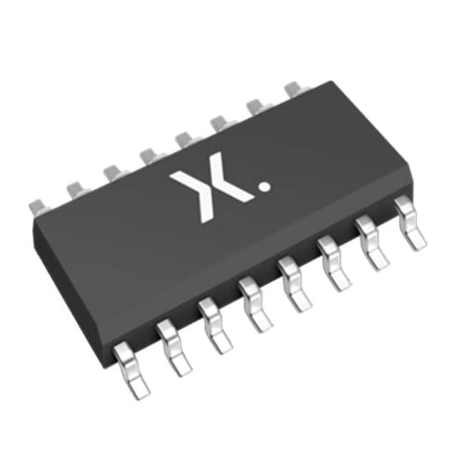
Vishay Siliconix DG201HSDY-T1

Part No.:
DG201HSDY-T1
Manufacturer:
Vishay Siliconix
Category:
Analog Switches, Multiplexers, Demultiplexers
Package:
16-SOIC (0.154", 3.90mm Width)
Datasheet:
AetrixDG201HSDY-T1.pdf
Description:
IC SWITCH SPST-NCX4 50OHM 16SOIC
Quantity:
Payment:
Payment
Shipping:
Shipping

Inventory:2,943

Please send an inquiry. Send us your inquiry, and we will respond immediately.

Part Number
Quantity*
Price
Name*
Company
Email*
Comments

Product details

Overview

DG201HSDY-T1 from Vishay Siliconix is a high-speed quad SPST CMOS analog switch designed for precision signal routing in data acquisition and sample-and-hold circuits. It delivers 38 ns turn-on time, 25 Ω on-resistance (dual-supply), 100 pA off-leakage, and TTL/CMOS logic compatibility - enabling fast, low-error switching of ±15 V analog signals in automated test equipment.

For engineers reviewing the DG201HSDY-T1 datasheet, DG201HSDY-T1 pinout, DG201HSDY-T1 application, or DG201HSDY-T1 equivalent, key selection criteria include guaranteed dual-supply operation up to ±15 V, channel-to-channel crosstalk of 100 dB at 100 kHz, 0.5 pF off-state drain-to-source capacitance, and TSSOP-16 packaging with RoHS-compliant terminations.

Technical Context

The DG201HSDY-T1 implements four independent bidirectional analog switches fabricated on a proprietary high-voltage silicon-gate process with epitaxial latchup protection. Each channel supports rail-to-rail analog signal ranges from V− to V+, with symmetrical conduction when ON and clamping diodes limiting input overvoltage beyond supply rails.

It operates from dual supplies (±15 V) or single supply (up to 16.5 V), with logic thresholds fixed at VINH ≥ 2.4 V and VINL ≤ 0.8 V. Dynamic performance is characterized with RL = 1 kΩ and CL = 35 pF, and charge injection is specified at −5 pC (dual-supply) for minimal pedestal error in integrator reset applications.

Key Specifications

ParameterValue and Actual Design Meaning
tON38 ns typical - enables sub-26 MHz sampling in high-throughput data acquisition systems
rDS(on)25 Ω max (V+ = 15 V, V− = −15 V) - ensures <0.1% gain error in 1 kΩ load interfaces
IS(off)100 pA max at ±15.5 V - reduces DC offset drift in precision integrators and choppers
OIRR85 dB at 100 kHz - suppresses coupling between active and inactive channels in multi-channel systems
CDS(off)0.5 pF - minimizes feedthrough during fast digital transitions in communication signal paths
Q (Charge Injection)−5 pC (CL = 1 nF, VS = 0 V) - limits voltage step error to <5 mV in 1 µF hold capacitors
Supply Range±15 V dual or 10.8–16.5 V single - supports legacy ±15 V instrumentation and modern single-rail designs

Pinout & Package

Package: 16-pin TSSOP (4.4 mm × 5.0 mm, 0.65 mm pitch), RoHS-compliant, moisture sensitivity level 1.

Pin/TerminalCircuit RoleDesign Meaning
1, 5, 10, 15Digital Input (IN1–IN4)Active-high control lines compatible with TTL/CMOS logic; drive internal gate drivers
2, 3, 14, 13Source Terminals (S1–S4)Analog inputs/outputs; bidirectional, rail-to-rail capable (V− to V+)
4, 6, 12, 11Drain Terminals (D1–D4)Analog inputs/outputs; electrically identical to S pins; no polarity dependency
7V−Negative supply rail; must be connected for dual-supply operation or grounded for single-supply mode
16V+Positive supply rail; supplies internal bias and switch driver circuitry
8GNDAnalog/digital reference ground; decoupling capacitor required near pin
9NCNo connect - internally unconnected; must remain floating or tied to GND per layout guidelines

Key Features

FeatureDesign Value
High-Speed Switching38 ns tON enables real-time multiplexing in >25 MSPS data acquisition without timing bottlenecks
Low On-Resistance Match3% rDS(on) matching across channels ensures consistent gain and phase response in multi-path signal conditioning
Ultra-Low Leakage100 pA off-leakage preserves long time-constant accuracy in sample-and-hold and integrator reset circuits
Bidirectional Signal PathIdentical rDS(on) and CDS(off) in either direction simplifies PCB routing and eliminates signal flow assumptions
Overvoltage ClampingIntegrated diodes clamp S/D/IN pins to V+ or V− rails, protecting downstream circuitry from ±4 V transients

Applications

Data Acquisition SystemsSample-and-Hold Circuits

Use Scenario: Multiplexing multiple sensor inputs into a shared ADC in aerospace telemetry units.

IC Role / Device Role / Timing Role: Quad SPST analog switch providing channel isolation and fast settling before conversion.

Use Value: 38 ns tON and 100 pA leakage ensure <0.01% measurement error across 16-bit dynamic range at 1 MSPS.

Use Scenario: Resetting integrator capacitors in precision analog computing modules.

IC Role / Device Role / Timing Role: Low-charge-injection switch discharging hold capacitors without pedestal error.

Use Value: −5 pC charge injection limits residual voltage to <5 mV on 1 µF capacitors, preserving DC accuracy.

Automatic Test EquipmentAvionics Signal Routing

Use Scenario: Reconfiguring stimulus/sense paths across DUTs in modular PXI chassis.

IC Role / Device Role / Timing Role: High-isolation (85 dB OIRR), low-crosstalk (100 dB) switch matrix element.

Use Value: 0.5 pF CDS(off) and 100 dB XTalk prevent false triggering and crosstalk-induced measurement noise.

Use Scenario: Routing analog sensor outputs (pitot, temperature, gyro) to redundant flight computers.

IC Role / Device Role / Timing Role: Radiation-tolerant analog switch supporting MIL-STD-883 Class B screening (D suffix).

Use Value: −40 °C to +85 °C operating range and latchup-immune epitaxial process ensure reliability in airborne environments.

Equivalent & Alternatives

The following parts are listed as comparable options for similar quad SPST analog switch applications.

Alternative PartTechnical DifferenceApplication DifferenceSelection Advice
ADG201HSSame pinout, identical electrical specs; discontinued by Analog Devices; last-time-buy statusNo functional difference; requires qualification for long-term production continuitySelect DG201HSDY-T1 for assured supply and Vishay's extended lifecycle support
HI201HSLegacy Intersil part; higher rDS(on) (35 Ω), slower tON (55 ns), no RoHS optionNot suitable for new designs requiring low power or lead-free complianceChoose DG201HSDY-T1 for improved speed, lower on-resistance, and full RoHS compliance

Compared with ADG201HS and HI201HS, the DG201HSDY-T1 offers identical functionality with enhanced manufacturability, guaranteed RoHS compliance, and superior dynamic performance - making it the preferred choice for new designs and obsolescence mitigation programs.

Availability

DG201HSDY-T1 is available at Aetrix Electronics and suitable for data acquisition systems, avionics signal routing, and automatic test equipment requiring stable component supply, long-term lifecycle assurance, and RoHS-compliant packaging.

Supply support for DG201HSDY-T1 includes scheduled delivery planning, volume procurement assistance, BOM continuity management, traceable sourcing, and lifecycle availability coordination for OEM customers, industrial embedded developers, connected-device designers, and electronics production programs.

Manufacturer

Vishay Siliconix is a global leader in discrete semiconductors and passive components, specializing in high-reliability analog switching, power management, and sensing solutions.

The DG201HS product line targets high-speed, low-error analog signal routing in mission-critical instrumentation - emphasizing rail-to-rail operation, ultra-low leakage, and robust latchup immunity for aerospace, defense, and industrial test systems.

FAQ

What is the maximum analog signal voltage range supported by the DG201HSDY-T1?

The DG201HSDY-T1 supports analog signals from V− to V+ across all four channels. With ±15 V dual supplies, this yields a full −15 V to +15 V range. In single-supply mode (V− = GND), the range is 0 V to V+ (up to 16.5 V). Internal clamping diodes limit input excursions to (V− − 4 V) and (V+ + 4 V), protecting the device from transient overvoltage.

Does the DG201HSDY-T1 require external pull-up or pull-down resistors on its digital control inputs?

No, the DG201HSDY-T1 does not require external pull-up or pull-down resistors. Its digital inputs are TTL/CMOS compatible with defined thresholds: VINH ≥ 2.4 V for logic high and VINL ≤ 0.8 V for logic low. The input current remains within ±1 µA across temperature, allowing direct connection to microcontroller GPIO or FPGA outputs without additional biasing.

Can the DG201HSDY-T1 operate reliably in single-supply configurations?

Yes, the DG201HSDY-T1 is fully specified for single-supply operation from 10.8 V to 16.5 V with V− tied to GND. In this mode, the analog signal range is 0 V to V+, on-resistance increases to 65 Ω (typ), and turn-on time is 50 ns (typ). All timing, leakage, and isolation parameters remain guaranteed per the datasheet's single-supply specification table.

What is the thermal derating behavior of the DG201HSDY-T1 above 75 °C?

Above 75 °C, the DG201HSDY-T1's power dissipation must be linearly derated at 7.6 mW/°C for the TSSOP package. At 100 °C ambient, the allowable power drops from 600 mW (at ≤75 °C) to 409 mW. This derating ensures junction temperature remains within safe limits under continuous operation and maintains parameter stability per the datasheet's thermal characteristics.

How does the DG201HSDY-T1 handle overvoltage conditions on its analog terminals?

The DG201HSDY-T1 incorporates internal clamping diodes on all S, D, and IN pins. Signals exceeding (V− − 4 V) or (V+ + 4 V) forward-bias these diodes, diverting current to the supply rails. To avoid damage, forward diode current must be limited to the absolute maximum rating of 30 mA continuous or 100 mA pulsed (1 ms, 10% duty cycle), typically enforced via series resistors in the signal path.

DG201HSDY-T1 Specifications

Product attributes
Attribute value
Manufacturer:
Vishay Siliconix
Series:
-
Packaging:
Tape & Reel (TR)
Product Status:
Obsolete
Switch Circuit:
SPST - NC
Multiplexer/Demultiplexer Circuit:
1:1
Number of Circuits:
4
On-State Resistance (Max):
50Ohm
Channel-to-Channel Matching (ΔRon):
1.5Ohm
Voltage - Supply, Single (V+):
13V ~ 36V
Voltage - Supply, Dual (V±):
±7V ~ 22V
Switch Time (Ton, Toff) (Max):
60ns, 50ns
-3db Bandwidth:
-
Charge Injection:
-5pC
Channel Capacitance (CS(off), CD(off)):
5pF
Current - Leakage (IS(off)) (Max):
1nA
Crosstalk:
-100dB @ 100kHz
Operating Temperature:
-40°C ~ 85°C (TA)
Grade:
-
Qualification:
-
Mounting Type:
Surface Mount
Supplier Device Package:
16-SOIC

DG201HSDY-T1 FAQ

1.How can I place an order for DG201HSDY-T1 through Aetrix?

Please submit a Request for Quotation (RFQ) for DG201HSDY-T1 on Aetrix. Our sales agent will provide a competitive quotation and guide you through the order confirmation once you accept the terms.

2.Are the price and stock information for DG201HSDY-T1 reliable?

The price and inventory of DG201HSDY-T1 are updated periodically and may fluctuate due to market conditions. Stock and pricing data are typically refreshed every 24 hours. Quotation validity for DG201HSDY-T1 is usually 5 days.

3.What payment methods are accepted for DG201HSDY-T1?

We accept Wire Transfer, PayPal, Credit Card, Western Union, MoneyGram, and Escrow for DG201HSDY-T1 transactions.

Note: Certain payment methods may incur a processing fee.

4.How is shipping managed for DG201HSDY-T1?

DG201HSDY-T1 orders can be shipped via leading logistics carriers, including DHL, UPS, FedEx, TNT, or Registered Mail.

Once your DG201HSDY-T1 order is processed, you will receive an email with the shipment details and tracking number.

Note: Tracking information may take up to 24 hours to appear. Express delivery typically takes 3–5 business days.

5.How can I obtain technical support or documentation for DG201HSDY-T1?

For technical support, including DG201HSDY-T1 datasheets, pinout diagrams, or application guidance, please contact our engineering support team. They can provide detailed documentation and assistance for your DG201HSDY-T1 requirements.

6.How does Aetrix verify that DG201HSDY-T1 is sourced from the original manufacturer or authorized distributors?

All DG201HSDY-T1 products on Aetrix are procured from qualified distributors and authorized channels. Our dedicated quality assurance team conducts strict verification, including traceability checks and, if necessary, third-party testing. This ensures that DG201HSDY-T1 meets industry standards.

7.What is the process for return or replacement of DG201HSDY-T1?

All DG201HSDY-T1 units undergo pre-shipment inspection (PSI). If there is an issue with DG201HSDY-T1, returns or replacements are accepted under the following conditions:

1.Quantity discrepancies, incorrect items, or visible external defects (such as breakage or corrosion), acknowledged by Aetrix.

2.The issue is reported within 90 days of delivery.

3.The DG201HSDY-T1 part is unused and in its original packaging.

Return procedure for DG201HSDY-T1:

1.Submit a request within 90 days.

2.Obtain a Return Material Authorization (RMA) from Aetrix.

DG201HSDY-T1 Tags

  • DG201HSDY-T1
  • DG201HSDY-T1 PDF
  • DG201HSDY-T1 Datasheet
  • DG201HSDY-T1 Specifications
  • DG201HSDY-T1 Images
  • Vishay Siliconix
  • Vishay Siliconix DG201HSDY-T1
  • Buy DG201HSDY-T1
  • DG201HSDY-T1 Price
  • DG201HSDY-T1 Distributor
  • DG201HSDY-T1 Supplier
  • DG201HSDY-T1 Wholesale
Related Products
SN74LVC1G3157DBVR
SN74LVC1G3157DBVR

Texas Instruments

SN74LVC1G66DBVR
SN74LVC1G66DBVR

Texas Instruments

SN74LVC1G66DCKR
SN74LVC1G66DCKR

Texas Instruments

SN74LVC1G3157DSFR
SN74LVC1G3157DSFR

Texas Instruments

1P1G3157QDCKRQ1
1P1G3157QDCKRQ1

Texas Instruments

SN74LVC2G66DCUR
SN74LVC2G66DCUR

Texas Instruments

SN74LV4052APWR
SN74LV4052APWR

Texas Instruments

74HC4051D,653
74HC4051D,653

Nexperia USA Inc.

SN74LV4051APWR
SN74LV4051APWR

Texas Instruments

CD74HC4052PWR
CD74HC4052PWR

Texas Instruments

CD74HC4051PWR
CD74HC4051PWR

Texas Instruments

TS5A3166DBVR
TS5A3166DBVR

Texas Instruments

Tech Hub

Search

Search

PRODUCT

PRODUCT

PHONE

PHONE

USER

USER