Send an Inquiry

To receive a quote for your project, please fill in the following information, and we’ll get back to you promptly.

Name*
Company*
Email Address*
Phone/WhatsApp
Part Number*
Quantity*
Message
Submit Inventory List

Please fill in the following information, and we’ll get back to you promptly.

Name*
Company*
Email Address*
Phone/WhatsApp
Upload My List
Message

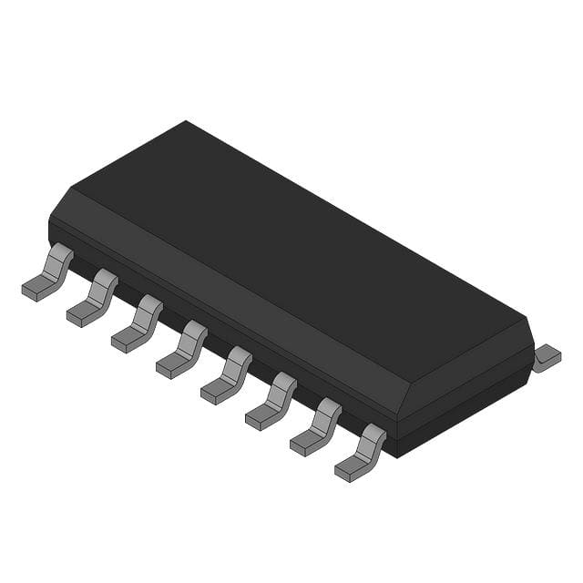
Vishay Siliconix DG413DY

Part No.:
DG413DY
Manufacturer:
Vishay Siliconix
Category:
Analog Switches, Multiplexers, Demultiplexers
Package:
16-SOIC (0.154", 3.90mm Width)
Datasheet:
AetrixDG413DY.pdf
Description:
IC SW SPST-NO/NCX4 35OHM 16SOIC
Quantity:
Payment:
Payment
Shipping:
Shipping

Inventory:1,316

Please send an inquiry. Send us your inquiry, and we will respond immediately.

Part Number
Quantity*
Price
Name*
Company
Email*
Comments

Product details

Overview

DG413DY from Vishay Siliconix is a precision monolithic quad SPST analog switch IC with two normally open (NO) and two normally closed (NC) switches, 44 V supply rating, 15 V analog signal range, 25 Ω typical on-resistance at ±15 V supplies, and 110 ns turn-on time-used in precision data acquisition systems requiring break-before-make switching action.

For engineers reviewing the DG413DY datasheet, DG413DY pinout, DG413DY application, or DG413DY equivalent, key selection criteria include dual logic polarity support (SW1/SW4 active-high, SW2/SW3 active-low), ±15 V or 12 V single-supply operation, low 5 pC charge injection, and SOIC-16 packaging for space-constrained industrial instrumentation.

Technical Context

The DG413DY implements four independent CMOS transmission gates fabricated on a high-voltage silicon gate process with epitaxial latchup protection. Its internal logic decodes two digital inputs to drive two NO and two NC switches simultaneously, enabling break-before-make timing with 25 ns guaranteed delay between channel transitions.

It supports bipolar (±15 V) and unipolar (12 V) supply configurations, where VL is tied to V+ in single-supply mode. Analog signal handling is symmetrical-each switch conducts bidirectionally with full rail-to-rail voltage blocking when off, and maintains <0.25 nA leakage across –40°C to +85°C.

Key Specifications

ParameterValue and Actual Design Meaning
Analog Signal Range±15 V - supports full-range signal switching without clipping in dual-supply precision systems
rDS(on) Typ.25 Ω at ±15 V - ensures minimal signal attenuation and gain error in sensor front-ends
tON / tOFF110 ns / 100 ns - enables sub-microsecond multiplexing in high-speed data loggers
Charge Injection5 pC - limits output voltage step errors in sample-and-hold or integrator circuits
OIRR68 dB - provides strong isolation between active and inactive channels at 1 MHz
Supply Voltage Max44 V - allows robust operation in industrial environments with transient overvoltage
Logic CompatibilityTTL/CMOS - interfaces directly with microcontrollers and FPGAs without level-shifting

Pinout & Package

Package: 16-pin narrow SOIC (SOIC-16), 3.9 mm width, JEDEC MS-012AC compliant, rated for –40°C to +85°C operation.

Pin/TerminalCircuit RoleDesign Meaning
IN1, IN2, IN3, IN4Digital control inputsIN1/IN4 active-high drives SW1/SW4 ON; IN2/IN3 active-low drives SW2/SW3 ON
S1–S4Switch source terminalsConnect to analog signal sources; bidirectional conduction path when switch is closed
D1–D4Switch drain terminalsConnect to analog signal destinations; identical electrical behavior to Sx pins
V+, V–Analog supply railsSupport ±15 V dual supply or 12 V single supply (V– = GND); define analog signal swing limits
GNDGround referenceReturn path for logic and analog grounds; must be low-impedance for noise immunity
VLLogic supply inputAccepts 5 V TTL/CMOS logic levels; decoupled internally to prevent supply coupling into analog path

Key Features

FeatureDesign Value
Break-before-make switchingGuaranteed 25 ns minimum delay prevents momentary shorting between channels in multiplexer designs
Low on-resistance flatness±2 Ω variation over ±10 V signal range minimizes THD in audio and instrumentation paths
Ultra-low leakage±0.25 nA max off-leakage at full temperature range preserves accuracy in high-impedance sensor interfaces
Bidirectional analog conductionIdentical rDS(on) and capacitance in both directions simplifies PCB layout and signal routing
Single-supply capabilityOperates from 12 V with V– = GND and VL = V+, eliminating need for negative rail in portable systems

Applications

Precision Data AcquisitionAutomated Test Equipment (ATE)

Use Scenario: Multiplexing multiple sensor outputs (e.g., thermocouples, strain gauges) into a single ADC channel with minimal crosstalk and offset drift.

IC Role / Device Role / Timing Role: Quad SPST switch providing channel isolation and break-before-make sequencing to prevent signal contamination during switching.

Use Value: 68 dB off-isolation and 5 pC charge injection ensure <0.01% gain error and <1 LSB settling error in 16-bit systems.

Use Scenario: Routing calibration references and DUT signals within modular ATE rack systems requiring fast, repeatable switching.

IC Role / Device Role / Timing Role: Precision analog switch enabling sub-200 ns channel reconfiguration under microcontroller control.

Use Value: 110 ns tON and 100 ns tOFF support >1 MHz multiplexing rates while maintaining <0.5 mV switching glitch.

Battery-Powered InstrumentationIndustrial Process Monitoring

Use Scenario: Low-power handheld multimeter front-end selecting voltage, current, and resistance measurement paths.

IC Role / Device Role / Timing Role: Low-quiescent-power analog switch (0.35 W total) with dual logic polarity supporting flexible MCU interface schemes.

Use Value: 0.25 nA leakage and 25 Ω rDS(on) extend battery life while preserving measurement resolution down to µV levels.

Use Scenario: Isolating 4–20 mA loop sensors and RTD bridges in PLC I/O modules exposed to EMI and supply transients.

IC Role / Device Role / Timing Role: High-voltage-tolerant analog switch (44 V rating) with latchup-immune process for harsh factory-floor environments.

Use Value: Epitaxial layer prevents latchup; ±25 V GND-to-V– rating withstands common-mode surges without damage.

Equivalent & Alternatives

The following parts are listed as comparable options for similar quad SPST analog switch applications.

Alternative PartTechnical DifferenceApplication DifferenceSelection Advice
MAX4613CPD+Higher 45 Ω rDS(on), 130 ns tON, but offers fault-protection and overvoltage shutdownPreferred in safety-critical systems where input overvoltage may exceed ±20 VSelect MAX4613CPD+ only if fault protection is required; DG413DY delivers lower distortion in precision signal paths
ADG413BRZLower 20 Ω rDS(on), 100 ns tON, but requires separate VL and VDD pins and lacks LCC package optionBetter suited for new designs targeting lowest on-resistance and fastest switchingChoose ADG413BRZ for highest performance; DG413DY remains optimal for legacy SOIC-16 footprint compatibility and cost-sensitive volume production

Compared with MAX4613CPD+ and ADG413BRZ, the DG413DY balances proven reliability, SOIC-16 footprint compatibility, and optimized trade-offs among on-resistance, switching speed, and charge injection-making it ideal for established industrial data acquisition platforms where BOM stability and long-term sourcing matter.

Availability

DG413DY is available at Aetrix Electronics and suitable for precision data acquisition, automated test equipment, and battery-powered instrumentation requiring stable component supply and long-lifecycle support.

Supply support for DG413DY includes scheduled delivery planning, volume procurement assistance, BOM continuity management, traceable sourcing, and lifecycle availability coordination for OEM customers, industrial embedded developers, connected-device designers, and electronics production programs.

Manufacturer

Vishay Siliconix is a global semiconductor manufacturer specializing in discrete MOSFETs, analog switches, and high-reliability power components for industrial, military, and automotive markets.

The DG413DY belongs to the DG411/412/413 family of precision monolithic analog switches designed specifically for high-fidelity signal routing in test and measurement, instrumentation, and process control systems.

FAQ

What is the maximum supply voltage rating for the DG413DY?

The DG413DY supports up to 44 V across V+ and V– terminals, with absolute maximum ratings of ±25 V from GND to V– and V+ to V–. This wide supply range enables operation in industrial environments with significant rail transients, and allows use with 12 V single-supply or ±15 V dual-supply configurations without external regulation. The DG413DY maintains specified performance across its full rated supply range.

Does the DG413DY support single-supply operation?

Yes, the DG413DY supports true single-supply operation from 5 V to 44 V. In this mode, V– is connected to GND, V+ is tied to VL, and analog signals swing from 0 V to V+. The device is fully characterized at 12 V single supply, with rDS(on) ≤100 Ω and tON ≤400 ns over temperature. Logic thresholds scale with VL, ensuring reliable switching even at reduced supply voltages.

How does the DG413DY implement break-before-make switching?

The DG413DY integrates internal timing circuitry that guarantees a minimum 25 ns delay between turn-off of one switch pair and turn-on of the complementary pair (e.g., SW1 OFF before SW2 ON). This is explicitly verified per Figure 3 in the datasheet and ensures no momentary short-circuit occurs during channel transitions-critical for preventing signal corruption in multiplexer and relay-replacement applications using the DG413DY.

What is the charge injection specification for the DG413DY, and why does it matter?

The DG413DY specifies 5 pC typical charge injection at room temperature with CL = 10 nF. This parameter quantifies the net charge dumped onto the load capacitor during switching, directly causing voltage glitches in sample-and-hold, integrator, or filter circuits. At 5 pC, the resulting step error is <0.5 mV into a 10 nF capacitor-enabling accurate DC-coupled measurements in 16-bit data acquisition systems using the DG413DY.

Can the DG413DY be used in high-temperature industrial environments?

Yes, the DG413DY is rated for operation from –40°C to +85°C, with full parametric performance guaranteed across this range. Its high-voltage silicon gate process includes an epitaxial layer to prevent latchup, and leakage currents remain below ±0.25 nA even at +85°C. For extended temperature applications beyond +85°C, the DG413AK/883 variant (–55°C to +125°C) is available-but the standard DG413DY meets requirements for most industrial control and monitoring systems.

DG413DY Specifications

Product attributes
Attribute value
Manufacturer:
Vishay Siliconix
Series:
-
Packaging:
Tube
Product Status:
Obsolete
Switch Circuit:
SPST - NO/NC
Multiplexer/Demultiplexer Circuit:
1:1
Number of Circuits:
4
On-State Resistance (Max):
35Ohm
Channel-to-Channel Matching (ΔRon):
-
Voltage - Supply, Single (V+):
5V ~ 44V
Voltage - Supply, Dual (V±):
±5V ~ 20V
Switch Time (Ton, Toff) (Max):
175ns, 145ns
-3db Bandwidth:
-
Charge Injection:
5pC
Channel Capacitance (CS(off), CD(off)):
9pF, 9pF
Current - Leakage (IS(off)) (Max):
250pA
Crosstalk:
-85dB @ 1MHz
Operating Temperature:
-40°C ~ 85°C (TA)
Grade:
-
Qualification:
-
Mounting Type:
Surface Mount
Supplier Device Package:
16-SOIC

DG413DY FAQ

1.How can I place an order for DG413DY through Aetrix?

Please submit a Request for Quotation (RFQ) for DG413DY on Aetrix. Our sales agent will provide a competitive quotation and guide you through the order confirmation once you accept the terms.

2.Are the price and stock information for DG413DY reliable?

The price and inventory of DG413DY are updated periodically and may fluctuate due to market conditions. Stock and pricing data are typically refreshed every 24 hours. Quotation validity for DG413DY is usually 5 days.

3.What payment methods are accepted for DG413DY?

We accept Wire Transfer, PayPal, Credit Card, Western Union, MoneyGram, and Escrow for DG413DY transactions.

Note: Certain payment methods may incur a processing fee.

4.How is shipping managed for DG413DY?

DG413DY orders can be shipped via leading logistics carriers, including DHL, UPS, FedEx, TNT, or Registered Mail.

Once your DG413DY order is processed, you will receive an email with the shipment details and tracking number.

Note: Tracking information may take up to 24 hours to appear. Express delivery typically takes 3–5 business days.

5.How can I obtain technical support or documentation for DG413DY?

For technical support, including DG413DY datasheets, pinout diagrams, or application guidance, please contact our engineering support team. They can provide detailed documentation and assistance for your DG413DY requirements.

6.How does Aetrix verify that DG413DY is sourced from the original manufacturer or authorized distributors?

All DG413DY products on Aetrix are procured from qualified distributors and authorized channels. Our dedicated quality assurance team conducts strict verification, including traceability checks and, if necessary, third-party testing. This ensures that DG413DY meets industry standards.

7.What is the process for return or replacement of DG413DY?

All DG413DY units undergo pre-shipment inspection (PSI). If there is an issue with DG413DY, returns or replacements are accepted under the following conditions:

1.Quantity discrepancies, incorrect items, or visible external defects (such as breakage or corrosion), acknowledged by Aetrix.

2.The issue is reported within 90 days of delivery.

3.The DG413DY part is unused and in its original packaging.

Return procedure for DG413DY:

1.Submit a request within 90 days.

2.Obtain a Return Material Authorization (RMA) from Aetrix.

DG413DY Tags

  • DG413DY
  • DG413DY PDF
  • DG413DY Datasheet
  • DG413DY Specifications
  • DG413DY Images
  • Vishay Siliconix
  • Vishay Siliconix DG413DY
  • Buy DG413DY
  • DG413DY Price
  • DG413DY Distributor
  • DG413DY Supplier
  • DG413DY Wholesale
Related Products
SN74LVC1G3157DBVR
SN74LVC1G3157DBVR

Texas Instruments

SN74LVC1G66DBVR
SN74LVC1G66DBVR

Texas Instruments

SN74LVC1G66DCKR
SN74LVC1G66DCKR

Texas Instruments

SN74LVC1G3157DSFR
SN74LVC1G3157DSFR

Texas Instruments

1P1G3157QDCKRQ1
1P1G3157QDCKRQ1

Texas Instruments

SN74LVC2G66DCUR
SN74LVC2G66DCUR

Texas Instruments

SN74LV4052APWR
SN74LV4052APWR

Texas Instruments

74HC4051D,653
74HC4051D,653

Nexperia USA Inc.

SN74LV4051APWR
SN74LV4051APWR

Texas Instruments

CD74HC4052PWR
CD74HC4052PWR

Texas Instruments

CD74HC4051PWR
CD74HC4051PWR

Texas Instruments

TS5A3166DBVR
TS5A3166DBVR

Texas Instruments

Tech Hub

Search

Search

PRODUCT

PRODUCT

PHONE

PHONE

USER

USER