Send an Inquiry

To receive a quote for your project, please fill in the following information, and we’ll get back to you promptly.

Name*
Company*
Email Address*
Phone/WhatsApp
Part Number*
Quantity*
Message
Submit Inventory List

Please fill in the following information, and we’ll get back to you promptly.

Name*
Company*
Email Address*
Phone/WhatsApp
Upload My List
Message

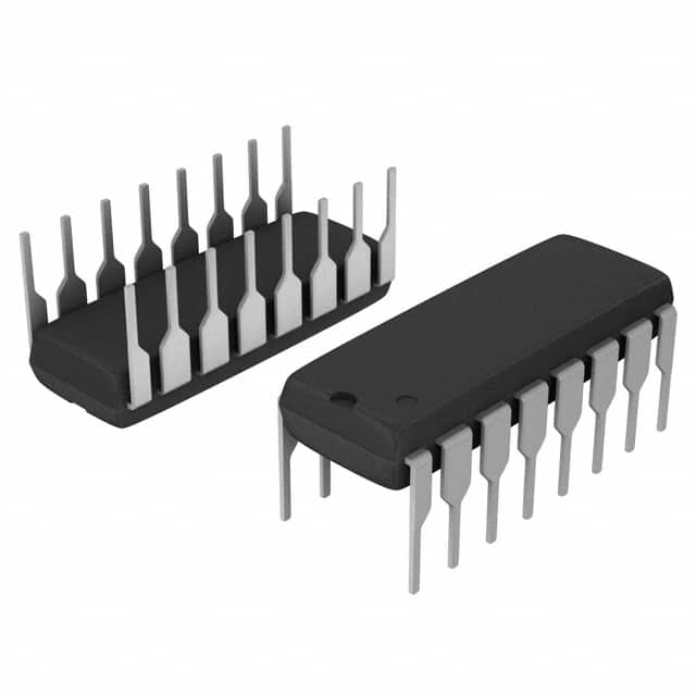
Vishay Siliconix DG441DJ-E3

Part No.:
DG441DJ-E3
Manufacturer:
Vishay Siliconix
Category:
Analog Switches, Multiplexers, Demultiplexers
Package:
16-DIP (0.300", 7.62mm)
Datasheet:
AetrixDG441DJ-E3.pdf
Description:
IC SWITCH SPST-NCX4 85OHM 16DIP
Quantity:
Payment:
Payment
Shipping:
Shipping

Inventory:2,808

Please send an inquiry. Send us your inquiry, and we will respond immediately.

Part Number
Quantity*
Price
Name*
Company
Email*
Comments

Product details

Overview

DG441DJ-E3 from Vishay Siliconix is a quad SPST analog switch with normally closed (NC) configuration, designed for high-speed, low-error switching of analog and audio signals in dual- or single-supply systems. It delivers 50 Ω typical on-resistance, 150 ns typical turn-on time, ±15 V dual-supply operation, and -1 pC charge injection - enabling precision sample-and-hold and data acquisition circuits.

For engineers reviewing the DG441DJ-E3 datasheet, DG441DJ-E3 pinout, DG441DJ-E3 application, or DG441DJ-E3 equivalent, key selection criteria include its NC logic behavior, low leakage (<0.5 nA off-state), TTL/CMOS-compatible control inputs, 16-pin plastic DIP package, and compatibility with legacy DG201A/DG202 socket upgrades.

Technical Context

The DG441DJ-E3 implements four independent, bidirectional SPST switches fabricated using Vishay's high-voltage silicon-gate process, featuring epitaxial latchup protection. Each channel conducts equally in both directions when on and blocks signals up to supply rails when off.

Its control logic is active-low for ON state (logic "0" ≤ 0.8 V enables conduction), with guaranteed switching across -40 °C to +85 °C. Charge injection is minimized at the drain terminal to reduce pedestal error in sampling applications, and internal clamping diodes protect against signal overvoltage beyond V+ or V−.

Key Specifications

ParameterValue and Actual Design Meaning
Switch TypeQuad SPST, normally closed (NC) - all four channels conduct when control input is logic low
On-Resistance50 Ω typ. at ±15 V supplies - ensures minimal signal attenuation and gain error in precision amplifiers
Turn-On Time150 ns typ. (RL = 1 kΩ, CL = 35 pF) - supports >1 MHz signal switching in data acquisition systems
Charge Injection-1 pC typ. - limits voltage step error in sample-and-hold circuits to <1 mV with 1 nF hold capacitor
Off-Leakage Current±0.5 nA max. at full temperature range - preserves accuracy in high-impedance sensor interfaces
Supply Range±5 V to ±22 V dual supply or +5 V to +36 V single supply - enables flexible rail design in industrial and medical equipment
Logic CompatibilityTTL/CMOS-compatible inputs (VIH ≥ 2.4 V, VIL ≤ 0.8 V) - simplifies interface with microcontrollers and FPGAs without level-shifting

Pinout & Package

Package: 16-pin plastic DIP (JEDEC MS-012), 0.300" wide body, lead pitch 0.100", RoHS-compliant (E3 suffix).

Pin/TerminalCircuit RoleDesign Meaning
1, 5, 9, 13IN1–IN4Active-low digital control inputs - logic "0" closes corresponding switch
2, 4, 11, 15S1–S4Source terminals - bidirectional analog signal entry points for each NC switch
3, 6, 12, 16D1–D4Drain terminals - bidirectional analog signal outputs; charge injection minimized here
7V−Negative supply rail - must be connected for dual-supply operation or grounded for single-supply use
8GNDAnalog/digital ground reference - shared return for supplies and logic
10, 14V+Positive supply rail - powers analog core and logic interface; supports up to +36 V
10, 14NCNo-connect pins - internally unused; must remain unconnected per datasheet

Key Features

FeatureDesign Value
Bidirectional analog conductionEnables signal routing in either direction without polarity constraints - ideal for multiplexing sensor inputs or audio paths
Low on-resistance match (≤5 Ω max)Ensures consistent gain and channel-to-channel tracking in programmable-gain amplifier designs
Clamped I/O with diode protectionPrevents damage from signals exceeding V+ or V− by limiting forward current - eliminates need for external clamps in ruggedized systems
Single-supply capability (+5 V to +36 V)Reduces system BOM count by eliminating negative rail generation in battery-powered or portable instrumentation
Epitaxial latchup immunityGuarantees robust operation under transient overvoltage or ESD stress - critical for medical and test equipment reliability

Applications

Audio SwitchingData Acquisition

Use Scenario: Routing line-level stereo signals between multiple sources and outputs in professional audio mixers.

IC Role / Device Role / Timing Role: Quad SPST NC switch providing silent, glitch-free channel selection with <150 ns transition.

Use Value: 50 Ω RDS(on) minimizes insertion loss; low charge injection prevents audible pop/click during switching.

Use Scenario: Multiplexing sensor outputs (thermocouples, strain gauges) into a shared ADC front-end.

IC Role / Device Role / Timing Role: Precision analog switch isolating high-impedance sources before sampling.

Use Value: ±0.5 nA off-leakage preserves microvolt-level signal integrity; 16 pF on-capacitance maintains bandwidth >1 MHz.

Sample-and-Hold CircuitsMedical Instrumentation

Use Scenario: Capturing transient physiological waveforms (ECG, EEG) with sub-microsecond aperture time control.

IC Role / Device Role / Timing Role: Normally closed switch acting as sampling gate, opened only during hold phase.

Use Value: -1 pC charge injection limits pedestal error to <100 µV with 1 nF hold capacitor - meets Class I medical accuracy requirements.

Use Scenario: Configurable gain and signal path selection in portable ultrasound or patient monitors.

IC Role / Device Role / Timing Role: Analog routing element enabling multi-range input scaling and calibration path switching.

Use Value: Dual-supply support (±15 V) accommodates bipolar transducer signals; latchup immunity ensures safety-critical reliability.

Equivalent & Alternatives

The following parts are listed as comparable options for similar analog switch applications.

Alternative PartTechnical DifferenceApplication DifferenceSelection Advice
MAX4617CPD+Quad SPST NO, 60 Ω RDS(on), 100 ns ton, requires external VEE for bipolar operationNot pin-compatible; NO logic requires inverted control signals vs. DG441DJ-E3's NC behaviorSelect when faster switching and lower on-resistance tolerance are prioritized over direct DG201A socket replacement
ADG441BNZQuad SPST NC, 45 Ω RDS(on), 120 ns ton, wider temp range (-40°C to +125°C), SOIC-16 onlySame NC function and pinout but different package - requires PCB redesign for DIP-16 footprintChoose for extended temperature operation and slightly better speed/resistance, accepting SOIC layout change

Compared with MAX4617CPD+ and ADG441BNZ, the DG441DJ-E3 offers verified DG201A socket compatibility, proven 16-pin DIP mechanical fit, and optimized charge injection for sample-and-hold - making it the preferred choice for legacy system upgrades and medical-grade precision analog routing where NC logic and DIP packaging are mandatory.

Availability

DG441DJ-E3 is available at Aetrix Electronics and suitable for audio switching, data acquisition, and medical instrumentation requiring stable component supply across long-lifecycle industrial programs.

Supply support for DG441DJ-E3 includes scheduled delivery planning, volume procurement assistance, BOM continuity management, traceable sourcing, and lifecycle availability coordination for OEM customers, industrial embedded developers, connected-device designers, and electronics production programs.

Manufacturer

Vishay Siliconix is a global leader in discrete semiconductors and passive components, specializing in high-reliability analog solutions for industrial, automotive, and medical markets.

The DG441DJ-E3 belongs to Vishay's high-voltage CMOS analog switch family, engineered specifically for precision signal routing in instrumentation-grade systems where low distortion, low leakage, and rail-to-rail signal handling are essential.

FAQ

What is the logic behavior of DG441DJ-E3?

The DG441DJ-E3 features normally closed (NC) SPST switches: each channel conducts when its INx pin is logic low (≤ 0.8 V) and opens when logic high (≥ 2.4 V). This active-low behavior matches legacy DG201A sockets and simplifies control in systems where default conduction is required during power-up or fault conditions. The DG441DJ-E3 does not require pull-up resistors for fail-safe operation.

Can DG441DJ-E3 operate from a single supply?

Yes, DG441DJ-E3 supports single-supply operation from +5 V to +36 V, with V− tied to GND. In this mode, analog signal range is 0 V to V+, and on-resistance increases to 100 Ω typ. (vs. 50 Ω typ. in ±15 V mode). The DG441DJ-E3 maintains TTL/CMOS compatibility and full functionality - making it suitable for battery-powered data loggers and portable medical devices.

What is the maximum signal voltage DG441DJ-E3 can switch?

The DG441DJ-E3 can switch analog signals from V− to V+ - i.e., ±15 V in dual-supply mode or 0 V to +12 V in single-supply mode. Absolute maximum ratings allow V+ to V− differential up to 44 V, but sustained signal excursion beyond supply rails is clamped by internal diodes. For reliable operation, keep signals within V− and V+ rails; the DG441DJ-E3 is not rated for overvoltage switching beyond these limits.

How does DG441DJ-E3 minimize errors in sample-and-hold circuits?

The DG441DJ-E3 minimizes sample-and-hold errors via ultra-low charge injection (-1 pC typ.) and low on-resistance (50 Ω typ.), which together limit pedestal voltage step and settling time. Its drain-terminal-optimized construction reduces injected charge directly into the hold capacitor, and the NC configuration allows seamless integration into open-loop S/H topologies like those shown in Vishay Application Note 826 - all confirmed in DG441DJ-E3 characterization data.

Is DG441DJ-E3 pin-compatible with DG201A?

Yes, DG441DJ-E3 is a direct drop-in upgrade for DG201A in 16-pin DIP sockets: identical pinout, NC logic, and mechanical footprint. It improves upon DG201A with 50 Ω vs. 90 Ω on-resistance, 150 ns vs. 350 ns turn-on time, and -1 pC vs. -5 pC charge injection - while maintaining backward compatibility. No PCB changes are required when replacing DG201A with DG441DJ-E3.

DG441DJ-E3 Specifications

Product attributes
Attribute value
Manufacturer:
Vishay Siliconix
Series:
-
Packaging:
Tube
Product Status:
Last Time Buy
Switch Circuit:
SPST - NC
Multiplexer/Demultiplexer Circuit:
1:1
Number of Circuits:
4
On-State Resistance (Max):
85Ohm
Channel-to-Channel Matching (ΔRon):
4Ohm (Max)
Voltage - Supply, Single (V+):
12V
Voltage - Supply, Dual (V±):
±15V
Switch Time (Ton, Toff) (Max):
220ns, 120ns
-3db Bandwidth:
-
Charge Injection:
-1pC
Channel Capacitance (CS(off), CD(off)):
4pF, 4pF
Current - Leakage (IS(off)) (Max):
500pA
Crosstalk:
-100dB @ 1MHz
Operating Temperature:
-40°C ~ 85°C (TA)
Grade:
-
Qualification:
-
Mounting Type:
Through Hole
Supplier Device Package:
16-PDIP

DG441DJ-E3 FAQ

1.How can I place an order for DG441DJ-E3 through Aetrix?

Please submit a Request for Quotation (RFQ) for DG441DJ-E3 on Aetrix. Our sales agent will provide a competitive quotation and guide you through the order confirmation once you accept the terms.

2.Are the price and stock information for DG441DJ-E3 reliable?

The price and inventory of DG441DJ-E3 are updated periodically and may fluctuate due to market conditions. Stock and pricing data are typically refreshed every 24 hours. Quotation validity for DG441DJ-E3 is usually 5 days.

3.What payment methods are accepted for DG441DJ-E3?

We accept Wire Transfer, PayPal, Credit Card, Western Union, MoneyGram, and Escrow for DG441DJ-E3 transactions.

Note: Certain payment methods may incur a processing fee.

4.How is shipping managed for DG441DJ-E3?

DG441DJ-E3 orders can be shipped via leading logistics carriers, including DHL, UPS, FedEx, TNT, or Registered Mail.

Once your DG441DJ-E3 order is processed, you will receive an email with the shipment details and tracking number.

Note: Tracking information may take up to 24 hours to appear. Express delivery typically takes 3–5 business days.

5.How can I obtain technical support or documentation for DG441DJ-E3?

For technical support, including DG441DJ-E3 datasheets, pinout diagrams, or application guidance, please contact our engineering support team. They can provide detailed documentation and assistance for your DG441DJ-E3 requirements.

6.How does Aetrix verify that DG441DJ-E3 is sourced from the original manufacturer or authorized distributors?

All DG441DJ-E3 products on Aetrix are procured from qualified distributors and authorized channels. Our dedicated quality assurance team conducts strict verification, including traceability checks and, if necessary, third-party testing. This ensures that DG441DJ-E3 meets industry standards.

7.What is the process for return or replacement of DG441DJ-E3?

All DG441DJ-E3 units undergo pre-shipment inspection (PSI). If there is an issue with DG441DJ-E3, returns or replacements are accepted under the following conditions:

1.Quantity discrepancies, incorrect items, or visible external defects (such as breakage or corrosion), acknowledged by Aetrix.

2.The issue is reported within 90 days of delivery.

3.The DG441DJ-E3 part is unused and in its original packaging.

Return procedure for DG441DJ-E3:

1.Submit a request within 90 days.

2.Obtain a Return Material Authorization (RMA) from Aetrix.

DG441DJ-E3 Tags

  • DG441DJ-E3
  • DG441DJ-E3 PDF
  • DG441DJ-E3 Datasheet
  • DG441DJ-E3 Specifications
  • DG441DJ-E3 Images
  • Vishay Siliconix
  • Vishay Siliconix DG441DJ-E3
  • Buy DG441DJ-E3
  • DG441DJ-E3 Price
  • DG441DJ-E3 Distributor
  • DG441DJ-E3 Supplier
  • DG441DJ-E3 Wholesale
Related Products
SN74LVC1G3157DBVR
SN74LVC1G3157DBVR

Texas Instruments

SN74LVC1G66DBVR
SN74LVC1G66DBVR

Texas Instruments

SN74LVC1G66DCKR
SN74LVC1G66DCKR

Texas Instruments

SN74LVC1G3157DSFR
SN74LVC1G3157DSFR

Texas Instruments

1P1G3157QDCKRQ1
1P1G3157QDCKRQ1

Texas Instruments

SN74LVC2G66DCUR
SN74LVC2G66DCUR

Texas Instruments

SN74LV4052APWR
SN74LV4052APWR

Texas Instruments

74HC4051D,653
74HC4051D,653

Nexperia USA Inc.

SN74LV4051APWR
SN74LV4051APWR

Texas Instruments

CD74HC4052PWR
CD74HC4052PWR

Texas Instruments

CD74HC4051PWR
CD74HC4051PWR

Texas Instruments

TS5A3166DBVR
TS5A3166DBVR

Texas Instruments

Tech Hub

Search

Search

PRODUCT

PRODUCT

PHONE

PHONE

USER

USER