
 My Inquiry
 My Account


Analog Devices Inc./Maxim Integrated DS1220AB-100IND
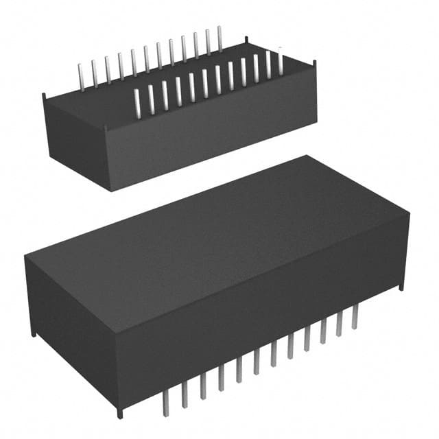
- Part No.:
- DS1220AB-100IND
- Manufacturer:
- Analog Devices Inc./Maxim Integrated
- Category:
- Memory
- Package:
- 24-DIP Module (0.600", 15.24mm)
- Datasheet:
-
 DS1220AB-100IND.pdf
- Description:
- IC NVSRAM 16KBIT PARALLEL 24EDIP
- Quantity:
- Payment:

- Shipping:

Inventory:4,504
Please send an inquiry. Send us your inquiry, and we will respond immediately.
Product details
Overview
DS1220AB-100IND from Maxim Integrated (now Analog Devices) is a 16k nonvolatile static RAM organized as 2048 × 8 bits, featuring lithium-backed data retention, 100 ns read/write access time, ±5% VCC tolerance (4.75–5.25 V), and industrial temperature operation (–40°C to +85°C). It directly replaces volatile 2k × 8 SRAMs and EEPROMs in legacy memory subsystems requiring power-loss immunity.
For engineers reviewing the DS1220AB-100IND datasheet, DS1220AB-100IND pinout, DS1220AB-100IND application, or DS1220AB-100IND equivalent, key selection criteria include guaranteed 10-year data retention without external power, automatic write protection during VCC decay, unlimited write cycles, JEDEC-standard 24-pin EDIP package compatibility, and seamless drop-in replacement for 2716 EPROM/2816 EEPROM footprints.
Technical Context
The DS1220AB-100IND integrates on-die lithium battery switching circuitry that monitors VCC continuously; when voltage falls below 4.5 V (VTP), it disables inputs, places outputs in high-Z, and connects the lithium source to retain RAM contents. During power-up, the switch disconnects the battery once VCC exceeds ~3.0 V and resumes normal CMOS SRAM operation above 4.75 V.
Its timing architecture supports asynchronous parallel bus interfacing with strict tACC = 100 ns, tWC = 100 ns, and tOE = 50 ns, while maintaining full compatibility with standard microprocessor control signals (CE, WE, OE) and address/data bus protocols used in 8-bit embedded systems and industrial controllers.
Key Specifications
| Parameter | Value and Actual Design Meaning |
|---|---|
| Memory Organization | 2048 words × 8 bits - matches byte-wide 2k × 8 SRAM footprint for direct PCB replacement |
| Access Time | 100 ns - enables integration into 10 MHz bus systems without wait states |
| VCC Range | 4.75 V to 5.25 V (±5%) - supports stable operation across regulated 5 V rails with typical tolerance drift |
| Data Retention | 10 years minimum without power - guaranteed by internal lithium cell and automatic backup switching |
| Operating Temperature | –40°C to +85°C - qualified for industrial control, metering, and automotive under-hood edge applications |
| Write Cycles | Unlimited - eliminates wear-out concerns in logging, configuration storage, or frequent state-save use cases |
| Package | 24-pin 720-mil extended DIP (EDIP) - JEDEC-standard through-hole footprint compatible with legacy 2716/2816 layouts |
Pinout & Package
DS1220AB-100IND uses a 24-pin 720-mil extended dual in-line package (EDIP) with through-hole mounting and RoHS-compliant lead finish. The package includes integrated lithium energy source and voltage-monitoring circuitry sealed within the epoxy body.
| Pin/Terminal | Circuit Role | Design Meaning |
|---|---|---|
| A0–A10 | Address Inputs | 11-bit address bus supporting full 2048-word addressing; TTL-compatible input thresholds |
| DQ0–DQ7 | Bi-directional Data I/O | 8-bit data bus with tristate output drivers; active only when CE and OE are asserted |
| CE | Chip Enable | Active-low chip select; initiates read/write when low; forces high-Z on power loss |
| WE | Write Enable | Active-low write strobe; controls data latching; disables outputs when asserted during reads |
| OE | Output Enable | Active-low output enable; isolates data bus during writes or standby to prevent contention |
| VCC | Power Supply | +5 V supply input; monitored for out-of-tolerance condition triggering automatic backup mode |
| GND | Ground Reference | System ground return; referenced for all DC and AC timing measurements |
Key Features
| Feature | Design Value |
|---|---|
| Lithium freshness seal | Battery remains electrically disconnected until first VCC application, preserving full 10-year retention capacity |
| Automatic write protection | Hardware-level VCC monitoring triggers unconditional write disable and high-Z outputs before data corruption occurs |
| Direct 2716/2816 pin compatibility | Identical pinout to 2716 EPROM and 2816 EEPROM - enables retrofit without PCB redesign |
| Zero support circuitry requirement | No external capacitors, regulators, or supervisory ICs needed for battery backup functionality |
| Industrial-grade reliability | Qualified over –40°C to +85°C with 100% tested AC/DC parameters and UL recognition (E99151) |
Applications
| Industrial Data Logger | Legacy PLC Memory Module |
|---|---|
Use Scenario: Continuous timestamped sensor readings stored during mains power interruption in factory-floor monitoring systems. IC Role / Device Role / Timing Role: Nonvolatile SRAM holding real-time operational state and last-valid measurement set during brownout events. Use Value: Eliminates need for external EEPROM write buffering and guarantees atomic state capture with no write-cycle delay or wear-out risk. | Use Scenario: Replacement memory for aging programmable logic controller backplanes originally using 2816 EEPROMs. IC Role / Device Role / Timing Role: Drop-in byte-wide memory device providing faster 100 ns access vs. 2816's 250+ ns and unlimited rewrites. Use Value: Enables deterministic scan-cycle timing and removes EEPROM erase/write latency bottlenecks in cyclic control execution. |
| Energy Meter Firmware Storage | Medical Device Configuration Backup |
Use Scenario: Storing tariff tables, calibration coefficients, and tamper-event logs in ANSI C12.20-compliant electricity meters. IC Role / Device Role / Timing Role: Secure, long-term configuration memory retaining critical billing parameters across 10+ year field deployment. Use Value: Meets 10-year data retention mandate without periodic refresh or external battery management circuitry. | Use Scenario: Preserving user-defined alarm thresholds, calibration offsets, and therapy settings in portable diagnostic equipment. IC Role / Device Role / Timing Role: Fail-safe memory element ensuring patient-critical configuration survives unexpected shutdown or battery swap. Use Value: Prevents clinical workflow disruption by guaranteeing immediate restore of validated settings post-power recovery. |
Equivalent & Alternatives
The following parts are listed as comparable options for similar nonvolatile SRAM applications.
| Alternative Part | Technical Difference | Application Difference | Selection Advice |
|---|---|---|---|
| DS1220AD-100IND+ | Wider VCC range (4.5–5.5 V, ±10%), lower VTP (4.25 V); otherwise identical pinout, timing, and retention | Suitable where input rail regulation is looser or brownout threshold must trigger earlier | Select DS1220AD-100IND+ if system VCC varies beyond ±5% or requires earlier backup activation |
| MAX6900AEN+ | Serial I²C interface, 16 kbit EEPROM architecture, no internal battery; requires external write-protection logic | Lower pin count (8-pin SO), but slower (5 ms write), limited endurance (~1M cycles), no automatic power-fail response | Choose MAX6900AEN+ only for space-constrained designs accepting serial interface overhead and reduced reliability |
Compared with DS1220AB-100IND, DS1220AD-100IND+ offers greater supply voltage flexibility at the cost of slightly reduced noise margin, while MAX6900AEN+ trades parallel bus performance and autonomous backup for compact packaging and simplified routing - neither provides true drop-in equivalence without firmware or layout changes.
Availability
DS1220AB-100IND is available at Aetrix Electronics and suitable for industrial data loggers, legacy PLC upgrades, and energy meter firmware storage requiring stable component supply, long-life data retention, and proven drop-in compatibility with 24-pin DIP memory sockets.
Supply support for DS1220AB-100IND includes scheduled delivery planning, volume procurement assistance, BOM continuity management, traceable sourcing, and lifecycle availability coordination for OEM customers, industrial embedded developers, connected-device designers, and electronics production programs.
Manufacturer
Maxim Integrated, now part of Analog Devices, designs precision analog, mixed-signal, and power management ICs for industrial, automotive, and communications applications.
The DS1220AB-100IND belongs to Maxim's nonvolatile SRAM product line, engineered specifically to replace aging EPROM/EEPROM memory in mission-critical systems where data integrity during power failure is non-negotiable.
FAQ
What is the guaranteed data retention period for DS1220AB-100IND?
The DS1220AB-100IND guarantees a minimum 10-year data retention period in the absence of external power, measured from the time VCC is first applied. This is achieved via an internal lithium energy source and automatic power-fail detection circuitry that switches to battery backup when VCC drops below 4.5 V. The retention time is design-guaranteed and not 100% tested per unit.
Does DS1220AB-100IND require external support components for battery backup operation?
No, DS1220AB-100IND requires no external support components for battery backup operation. Its integrated lithium cell and voltage-monitoring circuitry operate autonomously: the lithium source is electrically disconnected until first power-up, then automatically engages during VCC failure. No capacitors, supervisors, or regulators are needed for full nonvolatile functionality.
Is DS1220AB-100IND pin-compatible with standard 2716 EPROMs and 2816 EEPROMs?
Yes, DS1220AB-100IND has identical pinout and signal definitions to both the 2716 EPROM and 2816 EEPROM, enabling direct socket replacement in legacy systems. Address lines A0–A10, data lines DQ0–DQ7, and control signals CE, WE, OE, VCC, and GND map one-to-one, allowing hardware reuse without PCB modification.
What is the operating voltage range and tolerance specification for DS1220AB-100IND?
The DS1220AB-100IND operates over a VCC range of 4.75 V to 5.25 V, corresponding to a ±5% tolerance around nominal 5 V. Full functional operation-including read, write, and automatic backup activation-is specified across this range. Write protection triggers at VTP = 4.5 V to 4.75 V, ensuring robustness against marginal supply conditions.
How does DS1220AB-100IND handle power-down and power-up transitions?
During power-down, DS1220AB-100IND detects VCC decay below 4.5 V within 1.5 µs, disables all inputs, places outputs in high-Z, and connects the lithium source to RAM within 300 µs. At power-up, it reconnects VCC to RAM and disconnects the battery once VCC exceeds ~3.0 V, resuming full SRAM operation after VCC stabilizes above 4.75 V - all without software intervention.
DS1220AB-100IND Specifications
- Product attributes
- Attribute value
- Manufacturer:
- Analog Devices Inc./Maxim Integrated
- Series:
- -
- Package/Case:
- 24-DIP Module (0.600", 15.24mm)
- Packaging:
- Tube
- Product Status:
- Obsolete
- Programmable:
- Not Verified
- Memory Type:
- Non-Volatile
- Memory Format:
- NVSRAM
- Technology:
- NVSRAM (Non-Volatile SRAM)
- Memory Size:
- 16Kbit
- Memory Organization:
- 2K x 8
- Memory Interface:
- Parallel
- Clock Frequency:
- -
- Write Cycle Time - Word, Page:
- 100ns
- Access Time:
- 100 ns
- Voltage - Supply:
- 4.75V ~ 5.25V
- Operating Temperature:
- -40°C ~ 85°C (TA)
- Grade:
- -
- Qualification:
- -
- Mounting Type:
- Through Hole
- Supplier Device Package:
- 24-EDIP
DS1220AB-100IND FAQ
1.How can I place an order for DS1220AB-100IND through Aetrix?
Please submit a Request for Quotation (RFQ) for DS1220AB-100IND on Aetrix. Our sales agent will provide a competitive quotation and guide you through the order confirmation once you accept the terms.
2.Are the price and stock information for DS1220AB-100IND reliable?
The price and inventory of DS1220AB-100IND are updated periodically and may fluctuate due to market conditions. Stock and pricing data are typically refreshed every 24 hours. Quotation validity for DS1220AB-100IND is usually 5 days.
3.What payment methods are accepted for DS1220AB-100IND?
We accept Wire Transfer, PayPal, Credit Card, Western Union, MoneyGram, and Escrow for DS1220AB-100IND transactions.
Note: Certain payment methods may incur a processing fee.
4.How is shipping managed for DS1220AB-100IND?
DS1220AB-100IND orders can be shipped via leading logistics carriers, including DHL, UPS, FedEx, TNT, or Registered Mail.
Once your DS1220AB-100IND order is processed, you will receive an email with the shipment details and tracking number.
Note: Tracking information may take up to 24 hours to appear. Express delivery typically takes 3–5 business days.
5.How can I obtain technical support or documentation for DS1220AB-100IND?
For technical support, including DS1220AB-100IND datasheets, pinout diagrams, or application guidance, please contact our engineering support team. They can provide detailed documentation and assistance for your DS1220AB-100IND requirements.
6.How does Aetrix verify that DS1220AB-100IND is sourced from the original manufacturer or authorized distributors?
All DS1220AB-100IND products on Aetrix are procured from qualified distributors and authorized channels. Our dedicated quality assurance team conducts strict verification, including traceability checks and, if necessary, third-party testing. This ensures that DS1220AB-100IND meets industry standards.
7.What is the process for return or replacement of DS1220AB-100IND?
All DS1220AB-100IND units undergo pre-shipment inspection (PSI). If there is an issue with DS1220AB-100IND, returns or replacements are accepted under the following conditions:
1.Quantity discrepancies, incorrect items, or visible external defects (such as breakage or corrosion), acknowledged by Aetrix.
2.The issue is reported within 90 days of delivery.
3.The DS1220AB-100IND part is unused and in its original packaging.
Return procedure for DS1220AB-100IND:
1.Submit a request within 90 days.
2.Obtain a Return Material Authorization (RMA) from Aetrix.
DS1220AB-100IND Tags

-
M24C02-WMN6TP
STMicroelectronics

-
AT24C02C-XHM-T
Microchip Technology

-
AT21CS01-STUM10-T
Microchip Technology

-
AT24C02C-SSHM-T
Microchip Technology

-
24LC01BT-I/OT
Microchip Technology

-
M24C02-FMC6TG
STMicroelectronics
-
AT24CS02-SSHM-T
Microchip Technology

-
93LC46BT-I/OT
Microchip Technology
-
AT24C04C-SSHM-T
Microchip Technology

-
24LC01BT-I/SN
Microchip Technology
-
24AA02UIDT-I/OT
Microchip Technology

-
AT24C08C-STUM-T
Microchip Technology
Tech Hub

Comparator circuit design covering voltage thresholds, input limits, open-collector outputs, LM393 wiring, op-amp differences, hysteresis, timing, window detection and practical fault diagnosis.

Schmitt triggers use separate rising and falling thresholds to stabilize slow or noisy signals. This guide covers hysteresis, 74HC14 and 74HCT14 selection, comparator calculations, RC oscillators and p…

Counterfeit components can hide behind convincing markings and passing basic function tests. This engineering reference covers source traceability, external inspection, X-ray, XRF, electrical testing, …

A practical engineering and sourcing framework covering lifecycle verification, lifetime-buy calculations, replacement qualification, supplier checks and counterfeit-risk controls.

TTL and CMOS logic families differ in thresholds, loading, output drive, power and timing. This engineering guide compares 74HC and 74HCT, calculates noise margins and checks 3.3 V/5 V compatibility.

A practical engineering guide to 3.3V and 5V logic compatibility, input thresholds, resistor dividers, translator ICs, MOSFET level shifting, I2C pull-ups, timing limits and power-sequencing risks.

The 74HC595 uses push-pull logic outputs, while the TPIC6B595 uses 50 V open-drain DMOS sinks for higher-power loads. This guide compares timing, current limits, 3.3 V interfacing, load wiring, thermal…

The 74HC595 converts serial data into eight stable parallel outputs. This guide covers pin functions, shift and storage timing, OE and MR behavior, drive-current limits, cascading, voltage compatibilit…

A technical comparison of level-sensitive latches and edge-triggered flip-flops, covering timing windows, setup and hold limits, master–slave operation, time borrowing, race-through, HDL inference and…

A D latch stores one bit while Enable controls when data can pass. This reference covers gate-level operation, truth tables, transparency, setup and hold timing, LE versus OE, common ICs and practical …


