
 My Inquiry
 My Account


Analog Devices Inc./Maxim Integrated DS1225AD-200IND+
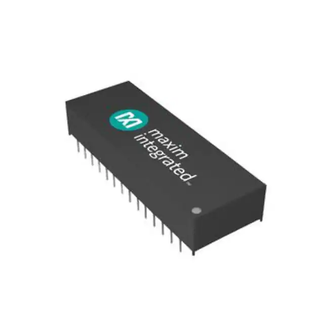
- Part No.:
- DS1225AD-200IND+
- Manufacturer:
- Analog Devices Inc./Maxim Integrated
- Category:
- Memory
- Package:
- 28-DIP Module (0.600", 15.24mm)
- Datasheet:
-
 DS1225AD-200IND+.pdf
- Description:
- IC NVSRAM 64KBIT PARALLEL 28EDIP
- Quantity:
- Payment:

- Shipping:

Inventory:1,117
Please send an inquiry. Send us your inquiry, and we will respond immediately.
Product details
Overview
DS1225AD-200IND+ from Maxim Integrated is a 64k-bit (8k × 8) nonvolatile static RAM with integrated lithium battery backup, JEDEC-standard 28-pin extended DIP package, 70 ns read/write access time, ±10% VCC tolerance (4.5V–5.5V), and industrial temperature range (–40°C to +85°C). It replaces volatile SRAMs or EEPROMs in embedded data-logging systems requiring zero-cycle write endurance and automatic power-loss protection.
For engineers reviewing the DS1225AD-200IND+ datasheet, DS1225AD-200IND+ pinout, DS1225AD-200IND+ application, or DS1225AD-200IND+ equivalent, key selection criteria include guaranteed 10-year data retention without external power, automatic VCC monitoring and write-protection activation below 4.25V, direct compatibility with 2764 EPROM/2864 EEPROM footprints, and no support circuitry required for microprocessor interfacing.
Technical Context
The DS1225AD-200IND+ integrates a self-contained lithium energy source and voltage-monitoring circuitry that continuously supervises VCC; when supply drops below 4.25V, it unconditionally enables write protection, disables inputs, and places outputs in high-impedance state before switching to battery power at ~3.0V. During power-up, the device reconnects VCC and disconnects the battery once VCC exceeds ~3.0V, resuming full operation above 4.5V.
It operates as a byte-wide parallel memory with standard SRAM timing: CE and OE low + WE high initiates read access; CE and WE low (with stable address) initiates write. All 13 address lines (A0–A12) and 8 bidirectional data lines (DQ0–DQ7) conform to JEDEC 28-pin DIP pinout, matching 2764/2864 devices for drop-in replacement in legacy designs.
Key Specifications
| Parameter | Value and Actual Design Meaning |
|---|---|
| Memory size | 65,536 bits (8,192 × 8), directly substituting 8k × 8 SRAM/EPROM/EEPROM |
| Access time | 70 ns tACC, enabling use with 14 MHz bus clocks without wait states |
| VCC operating range | 4.5V to 5.5V (±10%), supporting wide-tolerance industrial power rails |
| Data retention | Minimum 10 years without external power, guaranteed from first power-on |
| Write protection threshold | Activates automatically at VTP = 4.25V (min), preventing corruption during brownout |
| Temperature range | –40°C to +85°C (IND grade), qualified for harsh industrial environments |
| Package | 28-pin 720-mil extended DIP (EDIP), RoHS-compliant (indicated by "+" suffix) |
Pinout & Package
DS1225AD-200IND+ uses a JEDEC-standard 28-pin extended DIP (720-mil width) with internal lithium battery and power-switching circuitry. Pin assignments are fully compatible with 2764 EPROM and 2864 EEPROM footprints.
| Pin/Terminal | Circuit Role | Design Meaning |
|---|---|---|
| A0–A12 | Address inputs | 13-bit address bus for selecting one of 8,192 bytes; TTL-compatible inputs |
| DQ0–DQ7 | Bidirectional data I/O | 8-bit data bus with tristate outputs; active only when CE and OE are asserted |
| CE | Chip Enable | Active-low chip select; controls device enable and write-cycle initiation timing |
| WE | Write Enable | Active-low write strobe; combined with CE to define write cycle boundaries |
| OE | Output Enable | Active-low output control; enables data drivers during read cycles only |
| VCC | Power supply | +5V supply (4.5V–5.5V); powers logic and triggers battery disconnection on first power-up |
| GND | Ground reference | Signal and power return; must be connected before VCC during power-up |
| NC | No connect | Pins 14 and 24 are internally unused; must remain unconnected |
Key Features
| Feature | Design Value |
|---|---|
| Unlimited write cycles | Eliminates wear-out concerns in high-frequency logging applications; no write endurance limits |
| Automatic power-fail response | Sub-µs detection (tPD = 1.5 µs) and seamless switch to battery backup at ~3.0V |
| Freshness seal | Lithium source electrically disconnected until first VCC application, preserving full 10-year capacity |
| Direct EPROM/EEPROM replacement | Identical pinout and timing to 2764/2864, enabling hardware reuse without PCB changes |
| Low-power standby | ICCS2 = 3.0–5.0 mA at CE = VCC – 0.5V, reducing system-level quiescent consumption |
Applications
| Industrial Data Logger | Medical Device Memory |
|---|---|
Use Scenario: Standalone environmental sensor node recording temperature, pressure, and humidity every 5 seconds across multi-year deployments. IC Role / Device Role / Timing Role: Nonvolatile SRAM storing raw sensor data with atomic write capability and automatic save-on-power-loss. Use Value: Guarantees zero data loss during unexpected AC failure or battery depletion; eliminates need for external backup capacitors or supercapacitors. | Use Scenario: Portable ECG monitor capturing waveform snapshots during patient transport where mains power is unavailable. IC Role / Device Role / Timing Role: Primary data buffer retaining critical waveform segments during brief power interruptions or battery swaps. Use Value: Maintains clinical-grade data integrity without firmware intervention; meets IEC 60601-1 requirements for uninterrupted memory retention. |
| Avionics Black Box Recorder | PLC Configuration Storage |
Use Scenario: Flight data recorder capturing engine parameters, control surface positions, and navigation telemetry in commercial aircraft. IC Role / Device Role / Timing Role: High-reliability, radiation-tolerant (by design) memory holding last 30 minutes of flight data with deterministic save-on-failure. Use Value: Meets DO-160E Section 22 crash-survivable data retention requirements via autonomous battery switchover and write protection. | Use Scenario: Industrial programmable logic controller storing ladder logic programs, I/O mapping, and calibration constants across power cycles. IC Role / Device Role / Timing Role: Configuration memory retaining user-defined settings and runtime variables without EEPROM wear or slow write latency. Use Value: Enables instant restart after power loss; avoids 10ms+ EEPROM write delays and 100k-cycle endurance limits. |
Equivalent & Alternatives
The following parts are listed as comparable options for similar nonvolatile SRAM applications.
| Alternative Part | Technical Difference | Application Difference | Selection Advice |
|---|---|---|---|
| DS1225Y-70IND+ | Same 64k NV SRAM architecture but with ±5% VCC tolerance (4.75V–5.25V); lower VTP = 4.5V | Requires tighter-regulated 5V supply; less tolerant of brownout conditions than DS1225AD-200IND+ | Select when system already uses precision 5V regulators and industrial temp range is required |
| STK12C68-A70I | 64k NV SRAM with identical 28-pin DIP footprint and 70 ns speed, but uses different battery chemistry and write-protection threshold (4.4V) | Slightly higher write-protection voltage reduces usable brownout window vs. DS1225AD-200IND+ | Choose for second-source availability where DS1225AD-200IND+ lead times are constrained |
Compared with DS1225Y-70IND+ and STK12C68-A70I, DS1225AD-200IND+ offers the widest VCC operating margin (±10%) and lowest write-protection threshold (4.25V), maximizing robustness in fluctuating industrial power environments while maintaining full pin and timing compatibility.
Availability
DS1225AD-200IND+ is available at Aetrix Electronics and suitable for industrial data loggers, medical device memory buffers, avionics black box recorders, and PLC configuration storage requiring stable component supply, long-term lifecycle support, and guaranteed 10-year data retention.
Supply support for DS1225AD-200IND+ includes scheduled delivery planning, volume procurement assistance, BOM continuity management, traceable sourcing, and lifecycle availability coordination for OEM customers, industrial embedded developers, connected-device designers, and electronics production programs.
Manufacturer
Maxim Integrated (now part of Analog Devices) is a U.S.-based semiconductor company specializing in analog, mixed-signal, and high-reliability ICs for industrial, medical, and automotive markets.
The DS1225AB/AD product line delivers self-contained nonvolatile SRAM solutions designed for mission-critical data retention in systems where power interruption is unavoidable and firmware-based save routines are impractical.
FAQ
What is the guaranteed data retention period for DS1225AD-200IND+?
The DS1225AD-200IND+ guarantees minimum 10 years of data retention in the absence of external power, measured cumulatively from the time VCC is first applied. This specification is ensured by the sealed lithium energy source and internal power-switching circuitry, and applies across the full –40°C to +85°C industrial temperature range.
Does DS1225AD-200IND+ require external support circuitry for battery backup operation?
No, DS1225AD-200IND+ requires no external support circuitry. Its integrated lithium battery, voltage monitor, and power-switching logic operate autonomously. The device automatically disconnects the battery until first power-on (freshness seal), then monitors VCC continuously and switches to battery power within 1.5 µs when voltage falls below 4.25V.
Is DS1225AD-200IND+ pin-compatible with standard 2764 EPROMs?
Yes, DS1225AD-200IND+ uses the exact same 28-pin extended DIP footprint and pinout as the 2764 EPROM and 2864 EEPROM. Address lines (A0–A12), data lines (DQ0–DQ7), and control signals (CE, OE, WE, VCC, GND) align identically, enabling direct hardware substitution without PCB modification.
What is the write protection voltage threshold for DS1225AD-200IND+?
The DS1225AD-200IND+ activates unconditional write protection when VCC falls to 4.25V (minimum), with typical activation at 4.37V and maximum at 4.5V. This threshold is lower than the DS1225AB variant (4.5V min), providing extended operational margin during gradual brownout conditions.
Can DS1225AD-200IND+ operate with a 5V supply that varies between 4.5V and 5.5V?
Yes, DS1225AD-200IND+ is explicitly rated for VCC = 5V ±10%, meaning it operates reliably across 4.5V to 5.5V. Full functionality-including read/write access, standby current, and write-protection activation-is specified over this entire range, making it suitable for systems with unregulated or loosely regulated 5V rails.
DS1225AD-200IND+ Specifications
- Product attributes
- Attribute value
- Manufacturer:
- Analog Devices Inc./Maxim Integrated
- Series:
- -
- Package/Case:
- 28-DIP Module (0.600", 15.24mm)
- Packaging:
- Tube
- Product Status:
- Active
- Programmable:
- Not Verified
- Memory Type:
- Non-Volatile
- Memory Format:
- NVSRAM
- Technology:
- NVSRAM (Non-Volatile SRAM)
- Memory Size:
- 64Kbit
- Memory Organization:
- 8K x 8
- Memory Interface:
- Parallel
- Clock Frequency:
- -
- Write Cycle Time - Word, Page:
- 200ns
- Access Time:
- 200 ns
- Voltage - Supply:
- 4.5V ~ 5.5V
- Operating Temperature:
- -40°C ~ 85°C (TA)
- Grade:
- -
- Qualification:
- -
- Mounting Type:
- Through Hole
- Supplier Device Package:
- 28-EDIP
DS1225AD-200IND+ FAQ
1.How can I place an order for DS1225AD-200IND+ through Aetrix?
Please submit a Request for Quotation (RFQ) for DS1225AD-200IND+ on Aetrix. Our sales agent will provide a competitive quotation and guide you through the order confirmation once you accept the terms.
2.Are the price and stock information for DS1225AD-200IND+ reliable?
The price and inventory of DS1225AD-200IND+ are updated periodically and may fluctuate due to market conditions. Stock and pricing data are typically refreshed every 24 hours. Quotation validity for DS1225AD-200IND+ is usually 5 days.
3.What payment methods are accepted for DS1225AD-200IND+?
We accept Wire Transfer, PayPal, Credit Card, Western Union, MoneyGram, and Escrow for DS1225AD-200IND+ transactions.
Note: Certain payment methods may incur a processing fee.
4.How is shipping managed for DS1225AD-200IND+?
DS1225AD-200IND+ orders can be shipped via leading logistics carriers, including DHL, UPS, FedEx, TNT, or Registered Mail.
Once your DS1225AD-200IND+ order is processed, you will receive an email with the shipment details and tracking number.
Note: Tracking information may take up to 24 hours to appear. Express delivery typically takes 3–5 business days.
5.How can I obtain technical support or documentation for DS1225AD-200IND+?
For technical support, including DS1225AD-200IND+ datasheets, pinout diagrams, or application guidance, please contact our engineering support team. They can provide detailed documentation and assistance for your DS1225AD-200IND+ requirements.
6.How does Aetrix verify that DS1225AD-200IND+ is sourced from the original manufacturer or authorized distributors?
All DS1225AD-200IND+ products on Aetrix are procured from qualified distributors and authorized channels. Our dedicated quality assurance team conducts strict verification, including traceability checks and, if necessary, third-party testing. This ensures that DS1225AD-200IND+ meets industry standards.
7.What is the process for return or replacement of DS1225AD-200IND+?
All DS1225AD-200IND+ units undergo pre-shipment inspection (PSI). If there is an issue with DS1225AD-200IND+, returns or replacements are accepted under the following conditions:
1.Quantity discrepancies, incorrect items, or visible external defects (such as breakage or corrosion), acknowledged by Aetrix.
2.The issue is reported within 90 days of delivery.
3.The DS1225AD-200IND+ part is unused and in its original packaging.
Return procedure for DS1225AD-200IND+:
1.Submit a request within 90 days.
2.Obtain a Return Material Authorization (RMA) from Aetrix.
DS1225AD-200IND+ Tags

-
M24C02-WMN6TP
STMicroelectronics

-
AT24C02C-XHM-T
Microchip Technology

-
AT21CS01-STUM10-T
Microchip Technology

-
AT24C02C-SSHM-T
Microchip Technology

-
24LC01BT-I/OT
Microchip Technology

-
M24C02-FMC6TG
STMicroelectronics
-
AT24CS02-SSHM-T
Microchip Technology

-
93LC46BT-I/OT
Microchip Technology
-
AT24C04C-SSHM-T
Microchip Technology

-
24LC01BT-I/SN
Microchip Technology
-
24AA02UIDT-I/OT
Microchip Technology

-
AT24C08C-STUM-T
Microchip Technology
Tech Hub

Comparator circuit design covering voltage thresholds, input limits, open-collector outputs, LM393 wiring, op-amp differences, hysteresis, timing, window detection and practical fault diagnosis.

Schmitt triggers use separate rising and falling thresholds to stabilize slow or noisy signals. This guide covers hysteresis, 74HC14 and 74HCT14 selection, comparator calculations, RC oscillators and p…

Counterfeit components can hide behind convincing markings and passing basic function tests. This engineering reference covers source traceability, external inspection, X-ray, XRF, electrical testing, …

A practical engineering and sourcing framework covering lifecycle verification, lifetime-buy calculations, replacement qualification, supplier checks and counterfeit-risk controls.

TTL and CMOS logic families differ in thresholds, loading, output drive, power and timing. This engineering guide compares 74HC and 74HCT, calculates noise margins and checks 3.3 V/5 V compatibility.

A practical engineering guide to 3.3V and 5V logic compatibility, input thresholds, resistor dividers, translator ICs, MOSFET level shifting, I2C pull-ups, timing limits and power-sequencing risks.

The 74HC595 uses push-pull logic outputs, while the TPIC6B595 uses 50 V open-drain DMOS sinks for higher-power loads. This guide compares timing, current limits, 3.3 V interfacing, load wiring, thermal…

The 74HC595 converts serial data into eight stable parallel outputs. This guide covers pin functions, shift and storage timing, OE and MR behavior, drive-current limits, cascading, voltage compatibilit…

A technical comparison of level-sensitive latches and edge-triggered flip-flops, covering timing windows, setup and hold limits, master–slave operation, time borrowing, race-through, HDL inference and…

A D latch stores one bit while Enable controls when data can pass. This reference covers gate-level operation, truth tables, transparency, setup and hold timing, LE versus OE, common ICs and practical …


