
 My Inquiry
 My Account


Analog Devices Inc./Maxim Integrated DS1245Y-120
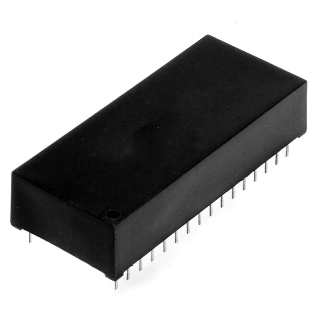
- Part No.:
- DS1245Y-120
- Manufacturer:
- Analog Devices Inc./Maxim Integrated
- Category:
- Memory
- Package:
- 32-DIP Module (0.600", 15.24mm)
- Datasheet:
-
 DS1245Y-120.pdf
- Description:
- IC NVSRAM 1MBIT PARALLEL 32EDIP
- Quantity:
- Payment:

- Shipping:

Inventory:4,512
Please send an inquiry. Send us your inquiry, and we will respond immediately.
Product details
Overview
DS1245Y-120 from Maxim Integrated is a 1024k (131,072 × 8) nonvolatile static RAM with lithium-backed data retention, ±10% VCC operation (4.5V–5.5V), 70 ns access time, and JEDEC-standard 32-pin DIP package. It replaces volatile SRAM, EEPROM, or Flash in systems requiring automatic write-protection during power loss - e.g., industrial PLCs preserving runtime configuration.
For engineers reviewing the DS1245Y-120 datasheet, DS1245Y-120 pinout, DS1245Y-120 application, or DS1245Y-120 equivalent, key selection criteria include guaranteed 10-year data retention without external power, self-contained lithium backup switching at ~3.0V, full functional operation down to 4.5V, and compatibility with legacy 128k×8 SRAM footprints.
Technical Context
The DS1245Y-120 integrates SRAM, lithium battery, and voltage-monitoring control circuitry into a single monolithic module. Its power-fail detection triggers unconditional write-protection and high-impedance outputs when VCC drops below 4.25V, then switches to battery power below ~3.0V.
It supports standard asynchronous parallel interface timing: read cycles require CE and OE low with WE high; write cycles require CE and WE low. Address inputs A0–A16 decode 131,072 locations; DQ0–DQ7 provide bidirectional 8-bit data transfer with tACC = 70 ns and tWC = 70 ns.
Key Specifications
| Parameter | Value and Actual Design Meaning |
|---|---|
| Memory Size | 1024 kbit (131,072 × 8) - matches 128k×8 SRAM footprint for drop-in replacement in legacy designs |
| Access Time | 70 ns - enables direct interfacing with 14 MHz microcontrollers without wait states |
| VCC Range | 4.5V to 5.5V (±10%) - supports wide-input industrial power rails without regulation overhead |
| Data Retention | 10 years minimum without external power - ensured by factory-sealed lithium cell activated only on first power-up |
| Write Protection Threshold | 4.25V - initiates automatic hardware lockout before brownout corrupts writes |
| Operating Temp | 0°C to +70°C (Commercial) - validated for stable operation in enclosed control cabinets |
| Package | 32-pin JEDEC 740-mil Extended DIP - compatible with wave-soldered PCBs and socket-based prototyping |
Pinout & Package
DS1245Y-120 uses a JEDEC-standard 32-pin Extended DIP (740-mil) package with integrated lithium battery and control logic. No external backup components are required.
| Pin/Terminal | Circuit Role | Design Meaning |
|---|---|---|
| A0–A16 | Address Inputs | 17-bit address bus supporting full 131,072-word addressing; TTL-compatible input thresholds |
| DQ0–DQ7 | Data I/O | Bidirectional 8-bit data bus; high-impedance during write or deselection to prevent bus contention |
| CE | Chip Enable | Active-low chip select; must be low for read/write; drives internal protection state during power fail |
| WE | Write Enable | Active-low write strobe; controls data latching and output disable during write cycles |
| OE | Output Enable | Active-low output enable; separates read timing from chip select for flexible bus arbitration |
| VCC | Power Supply | +5V supply pin; powers SRAM core and monitoring circuitry; disconnects lithium source above 4.25V |
| GND | Ground | Reference return for all signals and power; decoupling capacitor required near VCC/GND pins |
| NC | No Connect | Unbonded pins (pins 1, 17, 32); must remain unconnected per design - no routing or pull-ups |
Key Features
| Feature | Design Value |
|---|---|
| Automatic Power-Fail Write Protection | Hardware-enforced lockout triggered at 4.25V VCC, eliminating need for external supervisor ICs or firmware intervention |
| Lithium Freshness Seal | Factory-disconnected battery ensures full 10-year retention capacity; enabled only on first VCC application >4.25V |
| Unlimited Write Cycles | No endurance limit - supports continuous logging or real-time parameter updates without wear-out concerns |
| Self-Contained Nonvolatility | Single-package integration of SRAM, battery, and switch eliminates external capacitors, diodes, or backup controllers |
| Standard 32-Pin DIP Footprint | Direct replacement for obsolete 128k×8 volatile SRAMs (e.g., HM628128) without PCB redesign |
Applications
| Industrial Data Logger | Medical Device Configuration Storage |
|---|---|
|
Use Scenario: Battery-powered field logger records sensor readings every 5 seconds and retains last 72 hours of data across power interruptions. IC Role / Device Role / Timing Role: Nonvolatile SRAM providing immediate-read/write memory with zero-latency backup switching at 3.0V. Use Value: Eliminates supercapacitor charging delays and EEPROM write latency; guarantees atomic data preservation during grid flicker or battery swap. |
Use Scenario: Portable ultrasound unit stores user calibration profiles, probe settings, and safety limits that must survive overnight shutdown. IC Role / Device Role / Timing Role: Primary configuration memory with hardware write-protection activated before VCC falls below 4.25V. Use Value: Prevents corruption of critical medical parameters during unexpected AC loss; meets IEC 62304 data integrity requirements. |
| Telecom Base Station Clock Buffer | Automotive ECU Calibration Table Cache |
|
Use Scenario: Cellular base station maintains GPS timing offset tables and neighbor-cell handover parameters during brief utility outages. IC Role / Device Role / Timing Role: Low-access-time NVSRAM holding time-critical lookup tables accessed by FPGA timing controller. Use Value: Sustains synchronization accuracy without reacquisition delay; avoids 500ms+ GPS cold-start penalty after power recovery. |
Use Scenario: Engine control unit caches adaptive fuel trim values and knock sensor learning maps between ignition cycles. IC Role / Device Role / Timing Role: High-reliability memory storing dynamic calibration data updated every engine cycle. Use Value: Enables immediate torque delivery on restart; eliminates 3–5 second "limp mode" while EEPROM reloads calibration data. |
Equivalent & Alternatives
The following parts are listed as comparable options for similar nonvolatile SRAM applications.
| Alternative Part | Technical Difference | Application Difference | Selection Advice |
|---|---|---|---|
| DS1245AB-70+ | Narrower VCC range (4.75V–5.25V); higher write-protection threshold (4.50V) | Better suited for tightly regulated 5V systems where brownout margins exceed 5% | Select DS1245AB-70+ when system VCC ripple is <±2.5% and deterministic power-fail response above 4.5V is required. |
| STK12C68-AW50 | 50 ns access time; 3.3V/5V dual-supply support; different pinout (28-pin SOJ) | Requires PCB layout change; targets mixed-voltage embedded systems with faster timing needs | Choose STK12C68-AW50 only if 50 ns speed is mandatory and board redesign is acceptable. |
Compared with DS1245AB-70+, the DS1245Y-120 trades tighter voltage tolerance for broader compatibility with unregulated supplies, while STK12C68-AW50 offers speed and voltage flexibility at the cost of footprint incompatibility and no DIP option.
Availability
DS1245Y-120 is available at Aetrix Electronics and suitable for industrial data loggers, medical device configuration storage, and telecom timing buffer applications requiring stable component supply across extended product lifecycles.
Supply support for DS1245Y-120 includes scheduled delivery planning, volume procurement assistance, BOM continuity management, traceable sourcing, and lifecycle availability coordination for OEM customers, industrial embedded developers, connected-device designers, and electronics production programs.
Manufacturer
Maxim Integrated (now part of Analog Devices) designs precision analog, mixed-signal, and nonvolatile memory solutions for industrial, medical, and communications markets.
The DS1245Y-120 belongs to Maxim's nonvolatile SRAM family engineered for seamless replacement of volatile memory in systems where data integrity during power interruption is mission-critical.
FAQ
What is the guaranteed data retention period for DS1245Y-120 without external power?
The DS1245Y-120 guarantees a minimum of 10 years of data retention in the absence of external power. This is achieved using a factory-sealed lithium energy source that remains electrically disconnected until first application of VCC >4.25V, preserving full battery capacity. The 10-year figure is assured through component selection, process control, and design - not production-tested per unit.
Does DS1245Y-120 require external support circuitry for nonvolatile operation?
No, the DS1245Y-120 requires no external support circuitry for nonvolatile operation. It integrates the SRAM array, lithium battery, voltage-monitoring logic, and power-switching circuitry into a single 32-pin DIP package. Only standard VCC decoupling capacitance is needed - no supervisors, diodes, or backup capacitors are required.
What happens to DS1245Y-120 outputs during power failure?
When VCC falls below 4.25V, the DS1245Y-120 unconditionally enables write protection and places all outputs in high-impedance state within 1.5 µs. As VCC drops further to ~3.0V, the internal switch connects the lithium source to retain data. All address and data lines become "don't care," preventing bus conflicts during brownout.
Can DS1245Y-120 be used as a direct replacement for standard 128k×8 SRAMs?
Yes, the DS1245Y-120 uses a JEDEC-standard 32-pin 740-mil DIP footprint identical to legacy 128k×8 SRAMs like the HM628128. Its pinout (A0–A16, DQ0–DQ7, CE, WE, OE, VCC, GND) is fully compatible, enabling drop-in replacement without PCB modification - provided the system operates within its 4.5V–5.5V VCC range.
Is DS1245Y-120 RoHS-compliant and lead-free?
Yes, the DS1245Y-120 is RoHS-compliant and lead-free, indicated by the "+" suffix in its ordering code. It meets EU Directive 2011/65/EU and is manufactured using Maxim's lead(Pb)-free process. The package material is compatible with standard wave-soldering processes per JEDEC J-STD-020.
DS1245Y-120 Specifications
- Product attributes
- Attribute value
- Manufacturer:
- Analog Devices Inc./Maxim Integrated
- Series:
- -
- Package/Case:
- 32-DIP Module (0.600", 15.24mm)
- Packaging:
- Tube
- Product Status:
- Obsolete
- Programmable:
- Not Verified
- Memory Type:
- Non-Volatile
- Memory Format:
- NVSRAM
- Technology:
- NVSRAM (Non-Volatile SRAM)
- Memory Size:
- 1Mbit
- Memory Organization:
- 128K x 8
- Memory Interface:
- Parallel
- Clock Frequency:
- -
- Write Cycle Time - Word, Page:
- 120ns
- Access Time:
- 120 ns
- Voltage - Supply:
- 4.5V ~ 5.5V
- Operating Temperature:
- 0°C ~ 70°C (TA)
- Grade:
- -
- Qualification:
- -
- Mounting Type:
- Through Hole
- Supplier Device Package:
- 32-EDIP
DS1245Y-120 FAQ
1.How can I place an order for DS1245Y-120 through Aetrix?
Please submit a Request for Quotation (RFQ) for DS1245Y-120 on Aetrix. Our sales agent will provide a competitive quotation and guide you through the order confirmation once you accept the terms.
2.Are the price and stock information for DS1245Y-120 reliable?
The price and inventory of DS1245Y-120 are updated periodically and may fluctuate due to market conditions. Stock and pricing data are typically refreshed every 24 hours. Quotation validity for DS1245Y-120 is usually 5 days.
3.What payment methods are accepted for DS1245Y-120?
We accept Wire Transfer, PayPal, Credit Card, Western Union, MoneyGram, and Escrow for DS1245Y-120 transactions.
Note: Certain payment methods may incur a processing fee.
4.How is shipping managed for DS1245Y-120?
DS1245Y-120 orders can be shipped via leading logistics carriers, including DHL, UPS, FedEx, TNT, or Registered Mail.
Once your DS1245Y-120 order is processed, you will receive an email with the shipment details and tracking number.
Note: Tracking information may take up to 24 hours to appear. Express delivery typically takes 3–5 business days.
5.How can I obtain technical support or documentation for DS1245Y-120?
For technical support, including DS1245Y-120 datasheets, pinout diagrams, or application guidance, please contact our engineering support team. They can provide detailed documentation and assistance for your DS1245Y-120 requirements.
6.How does Aetrix verify that DS1245Y-120 is sourced from the original manufacturer or authorized distributors?
All DS1245Y-120 products on Aetrix are procured from qualified distributors and authorized channels. Our dedicated quality assurance team conducts strict verification, including traceability checks and, if necessary, third-party testing. This ensures that DS1245Y-120 meets industry standards.
7.What is the process for return or replacement of DS1245Y-120?
All DS1245Y-120 units undergo pre-shipment inspection (PSI). If there is an issue with DS1245Y-120, returns or replacements are accepted under the following conditions:
1.Quantity discrepancies, incorrect items, or visible external defects (such as breakage or corrosion), acknowledged by Aetrix.
2.The issue is reported within 90 days of delivery.
3.The DS1245Y-120 part is unused and in its original packaging.
Return procedure for DS1245Y-120:
1.Submit a request within 90 days.
2.Obtain a Return Material Authorization (RMA) from Aetrix.
DS1245Y-120 Tags

-
M24C02-WMN6TP
STMicroelectronics

-
AT24C02C-XHM-T
Microchip Technology

-
AT21CS01-STUM10-T
Microchip Technology

-
AT24C02C-SSHM-T
Microchip Technology

-
24LC01BT-I/OT
Microchip Technology

-
M24C02-FMC6TG
STMicroelectronics
-
AT24CS02-SSHM-T
Microchip Technology

-
93LC46BT-I/OT
Microchip Technology
-
AT24C04C-SSHM-T
Microchip Technology

-
24LC01BT-I/SN
Microchip Technology
-
24AA02UIDT-I/OT
Microchip Technology

-
AT24C08C-STUM-T
Microchip Technology
Tech Hub

Comparator circuit design covering voltage thresholds, input limits, open-collector outputs, LM393 wiring, op-amp differences, hysteresis, timing, window detection and practical fault diagnosis.

Schmitt triggers use separate rising and falling thresholds to stabilize slow or noisy signals. This guide covers hysteresis, 74HC14 and 74HCT14 selection, comparator calculations, RC oscillators and p…

Counterfeit components can hide behind convincing markings and passing basic function tests. This engineering reference covers source traceability, external inspection, X-ray, XRF, electrical testing, …

A practical engineering and sourcing framework covering lifecycle verification, lifetime-buy calculations, replacement qualification, supplier checks and counterfeit-risk controls.

TTL and CMOS logic families differ in thresholds, loading, output drive, power and timing. This engineering guide compares 74HC and 74HCT, calculates noise margins and checks 3.3 V/5 V compatibility.

A practical engineering guide to 3.3V and 5V logic compatibility, input thresholds, resistor dividers, translator ICs, MOSFET level shifting, I2C pull-ups, timing limits and power-sequencing risks.

The 74HC595 uses push-pull logic outputs, while the TPIC6B595 uses 50 V open-drain DMOS sinks for higher-power loads. This guide compares timing, current limits, 3.3 V interfacing, load wiring, thermal…

The 74HC595 converts serial data into eight stable parallel outputs. This guide covers pin functions, shift and storage timing, OE and MR behavior, drive-current limits, cascading, voltage compatibilit…

A technical comparison of level-sensitive latches and edge-triggered flip-flops, covering timing windows, setup and hold limits, master–slave operation, time borrowing, race-through, HDL inference and…

A D latch stores one bit while Enable controls when data can pass. This reference covers gate-level operation, truth tables, transparency, setup and hold timing, LE versus OE, common ICs and practical …


