
 My Inquiry
 My Account


Analog Devices Inc./Maxim Integrated DS1270AB-70IND
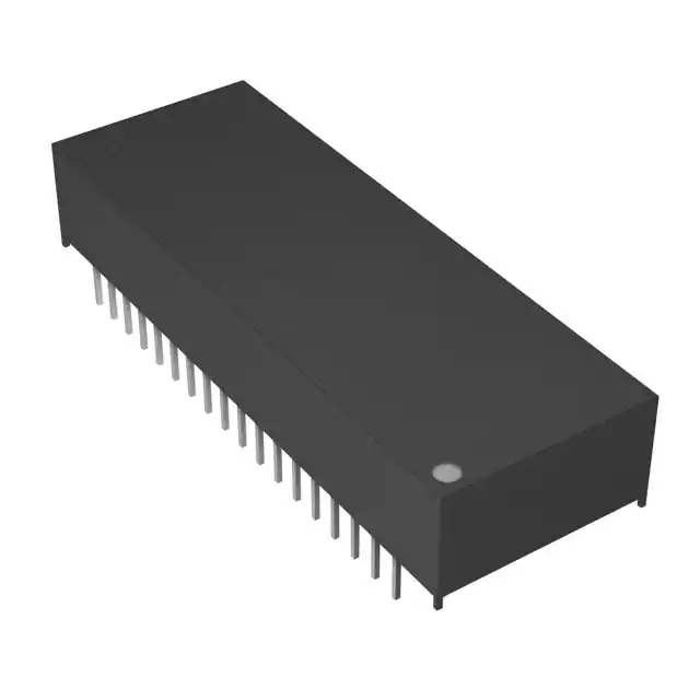
- Part No.:
- DS1270AB-70IND
- Manufacturer:
- Analog Devices Inc./Maxim Integrated
- Category:
- Memory
- Package:
- 36-DIP Module (0.610", 15.49mm)
- Datasheet:
-
 DS1270AB-70IND.pdf
- Description:
- IC NVSRAM 16MBIT PARALLEL 36EDIP
- Quantity:
- Payment:

- Shipping:

Inventory:1,867
Please send an inquiry. Send us your inquiry, and we will respond immediately.
Product details
Overview
DS1270AB-70IND from Maxim Integrated is a 16M-bit (2,097,152 × 8) nonvolatile static RAM with integrated lithium battery backup, 70 ns access time, ±5% VCC tolerance (4.75–5.25 V), and industrial temperature operation (–40°C to +85°C). It autonomously enables write protection and switches to battery power when VCC drops below 4.5 V, ensuring data integrity in power-loss scenarios such as industrial PLC memory retention.
For engineers reviewing the DS1270AB-70IND datasheet, DS1270AB-70IND pinout, DS1270AB-70IND application, or DS1270AB-70IND equivalent, key selection criteria include guaranteed 5-year data retention without external power, unlimited write cycles, full CMOS compatibility, and self-contained power-fail detection with no support circuitry required.
Technical Context
The DS1270AB-70IND implements a fully static NV SRAM architecture with on-chip voltage monitoring, automatic lithium source activation at ~3.0 V, and hardware-enforced write protection triggered at VTP = 4.50–4.75 V. Its control logic ensures CE/WE/OE timing compliance per JEDEC-standard parallel SRAM protocols.
All 21 address lines (A0–A20) and 8 bidirectional data lines (DQ0–DQ7) operate under strict DC and AC specifications: tACC = 70 ns, tWC = 70 ns, ICCS2 = 100–250 µA in standby, and VIL/VIH thresholds compatible with TTL and CMOS microcontrollers.
Key Specifications
| Parameter | Value and Actual Design Meaning |
|---|---|
| Memory Density | 16,777,216 bits (2,097,152 × 8) - supports byte-wide microprocessor interfaces without address decoding overhead |
| Access Time | 70 ns - enables direct connection to 14 MHz bus systems with zero wait states |
| VCC Range | 4.75 V to 5.25 V (±5%) - matches standard 5 V industrial power rails with margin for ripple |
| Data Retention | ≥5 years without external power - achieved via sealed lithium cell and automatic disconnect until first power-up |
| Operating Temp | –40°C to +85°C - qualified for embedded control in harsh environments including factory automation and energy metering |
| Write Protection Threshold | VTP = 4.50–4.75 V - initiates unconditional write lock before VCC reaches critical levels for SRAM stability |
| Standby Current | 100–250 µA at VCC–0.5 V - enables low-power hold mode during extended brownout conditions |
Pinout & Package
DS1270AB-70IND uses a 36-pin 740-mil Extended Dual In-line Package (EDIP), RoHS-compliant, wave- or hand-solderable only.
| Pin/Terminal | Circuit Role | Design Meaning |
|---|---|---|
| A0–A20 | Address Inputs | 21-bit address bus supporting full 2-Mbyte addressing; latched internally on CE/WE transitions |
| DQ0–DQ7 | Bidirectional Data I/O | CMOS-compatible 8-bit data path; high-impedance when OE inactive or during write cycles |
| CE | Chip Enable | Active-low chip select; must be stable before address setup; controls internal power state during power-down |
| WE | Write Enable | Active-low write strobe; determines write start/stop edges jointly with CE; disables outputs when asserted |
| OE | Output Enable | Active-low output control; enables read data drivers only when CE and WE are inactive |
| VCC | Power Supply | +5 V ±5% main supply; monitored continuously for fail-detect; powers RAM and control logic |
| GND | Ground | Reference return for all signals and internal switching circuits |
| NC | No Connect | Pins 13 and 24 - physically present but unconnected internally; must remain floating |
Key Features
| Feature | Design Value |
|---|---|
| Automatic Power-Fail Response | Switches to lithium backup and locks writes within 1.5 µs of VCC falling below VTP, preventing corruption during brownouts |
| Freshness Seal | Lithium source electrically disconnected until first VCC application > VTP, preserving full 5-year retention capacity |
| Unlimited Write Cycles | No endurance wear-out mechanism - supports continuous logging or configuration updates over product lifetime |
| Zero-Support-Logic Interface | Direct connection to 8-bit microcontrollers or FPGAs without glue logic, level shifters, or external supervisors |
| Industrial Temperature Qualification | Full AC/DC specs guaranteed across –40°C to +85°C, validated per Maxim's industrial reliability standards |
Applications
| Industrial PLC Data Logging | Smart Energy Meter Memory |
|---|---|
Use Scenario: Storing real-time energy consumption profiles and tariff schedules during grid outages. IC Role / Device Role / Timing Role: Nonvolatile SRAM holding meter firmware variables and billing data with autonomous power switchover. Use Value: Guarantees 5-year data retention without supercapacitors or external battery management, reducing BOM cost and board space. | Use Scenario: Maintaining tamper-proof event logs (e.g., lid opens, voltage sags) in utility-grade meters. IC Role / Device Role / Timing Role: Byte-addressable, write-protected memory that captures timestamped events even during rapid power loss. Use Value: Eliminates need for EEPROM wear-leveling algorithms and extends field life beyond 15 years with no write-cycle limits. |
| Railway Signaling Controller Memory | Medical Infusion Pump Configuration Storage |
Use Scenario: Preserving safety-critical operational parameters and fault history in wayside signaling units exposed to wide ambient swings. IC Role / Device Role / Timing Role: Industrial-temperature NV SRAM providing deterministic 70 ns read/write timing under EMI-heavy rail environments. Use Value: Meets EN 50121-3-2 immunity requirements by avoiding external clock sources or complex power sequencing. | Use Scenario: Storing calibrated dosing profiles, user preferences, and audit trails in battery-powered infusion devices. IC Role / Device Role / Timing Role: Low-quiescent-current (100–250 µA) nonvolatile memory enabling multi-year operation on primary cells. Use Value: Reduces standby current by >90% versus discrete SRAM + external supervisor solutions, extending battery service intervals. |
Equivalent & Alternatives
The following parts are listed as comparable options for similar nonvolatile SRAM applications.
| Alternative Part | Technical Difference | Application Difference | Selection Advice |
|---|---|---|---|
| DS1270Y-70IND | Wider VCC range (4.5–5.5 V, ±10%), lower VTP (4.25–4.5 V); otherwise identical pinout, timing, and retention | Better suited for systems with higher input ripple or legacy 5 V supplies lacking tight regulation | Select DS1270Y-70IND if VCC tolerance exceeds ±5%; DS1270AB-70IND preferred for tightly regulated 5 V rails |
| STK16C88-70I | Same density and 70 ns speed, but uses external capacitor-based backup; no integrated lithium; requires external supervisor | Lower component cost but adds design complexity, layout area, and qualification burden for backup circuitry | Choose STK16C88-70I only when lithium-free compliance (e.g., aviation transport) overrides reliability and integration benefits |
Compared with DS1270Y-70IND and STK16C88-70I, the DS1270AB-70IND delivers superior system-level simplicity through its self-contained lithium switch and tighter VCC window-reducing validation effort and eliminating external components while maintaining full industrial temperature performance.
Availability
DS1270AB-70IND is available at Aetrix Electronics and suitable for industrial PLC data logging, smart energy meter memory, and railway signaling controller memory requiring stable component supply, long-term lifecycle assurance, and RoHS-compliant sourcing.
Supply support for DS1270AB-70IND includes scheduled delivery planning, volume procurement assistance, BOM continuity management, traceable sourcing, and lifecycle availability coordination for OEM customers, industrial embedded developers, connected-device designers, and electronics production programs.
Manufacturer
Maxim Integrated (now part of Analog Devices) designs precision analog, mixed-signal, and power management ICs for industrial, automotive, and communications applications.
The DS1270AB-70IND belongs to Maxim's nonvolatile SRAM product line, engineered specifically for mission-critical memory retention in infrastructure equipment where power reliability cannot be assumed.
FAQ
What is the guaranteed data retention period for DS1270AB-70IND without external power?
The DS1270AB-70IND guarantees ≥5 years of data retention in the absence of external power, measured from the time VCC is first applied. This is achieved via an integrated, hermetically sealed lithium energy source that remains electrically disconnected until initial power-up, preserving full capacity. The specification is assured by component selection, process control, and design-not production-tested per unit.
Does DS1270AB-70IND require external circuitry to manage battery backup or power-fail detection?
No, DS1270AB-70IND requires no external circuitry. It integrates a voltage monitor, lithium power switch, and write-protection logic. When VCC falls below 4.5 V, it automatically disconnects the main supply, enables the lithium source, and places all inputs in "don't care" state and outputs in high-impedance-fully protecting data without support components.
What is the difference between DS1270AB-70IND and DS1270Y-70IND?
The DS1270AB-70IND operates over VCC = 4.75–5.25 V (±5%) with write protection activating at 4.50–4.75 V, while DS1270Y-70IND supports 4.5–5.5 V (±10%) and triggers protection at 4.25–4.5 V. Both share identical pinout, timing (70 ns), package, temperature range, and retention-making them functionally interchangeable where supply tolerance permits.
Can DS1270AB-70IND be used with microcontrollers that lack dedicated battery-backup control signals?
Yes, DS1270AB-70IND is designed for seamless integration with standard 8-bit microcontrollers. Its autonomous power-fail response eliminates the need for external interrupt signals, GPIO supervision, or software-driven backup enablement. The device handles all transitions-power-down, battery switchover, and power-up recovery-entirely in hardware.
Is DS1270AB-70IND RoHS-compliant and suitable for industrial reflow processes?
Yes, DS1270AB-70IND is RoHS-compliant (denoted by "#" suffix) and qualified for wave or hand soldering only. Its 36-pin 740-mil EDIP package is not rated for reflow due to internal lithium cell constraints; per Maxim's documentation, exposure to peak temperatures above 260°C or reflow profiles may compromise seal integrity and retention performance.
DS1270AB-70IND Specifications
- Product attributes
- Attribute value
- Manufacturer:
- Analog Devices Inc./Maxim Integrated
- Series:
- -
- Package/Case:
- 36-DIP Module (0.610", 15.49mm)
- Packaging:
- Tube
- Product Status:
- Obsolete
- Programmable:
- Not Verified
- Memory Type:
- Non-Volatile
- Memory Format:
- NVSRAM
- Technology:
- NVSRAM (Non-Volatile SRAM)
- Memory Size:
- 16Mbit
- Memory Organization:
- 2M x 8
- Memory Interface:
- Parallel
- Clock Frequency:
- -
- Write Cycle Time - Word, Page:
- 70ns
- Access Time:
- 70 ns
- Voltage - Supply:
- 4.75V ~ 5.25V
- Operating Temperature:
- -40°C ~ 85°C (TA)
- Grade:
- -
- Qualification:
- -
- Mounting Type:
- Through Hole
- Supplier Device Package:
- 36-EDIP
DS1270AB-70IND FAQ
1.How can I place an order for DS1270AB-70IND through Aetrix?
Please submit a Request for Quotation (RFQ) for DS1270AB-70IND on Aetrix. Our sales agent will provide a competitive quotation and guide you through the order confirmation once you accept the terms.
2.Are the price and stock information for DS1270AB-70IND reliable?
The price and inventory of DS1270AB-70IND are updated periodically and may fluctuate due to market conditions. Stock and pricing data are typically refreshed every 24 hours. Quotation validity for DS1270AB-70IND is usually 5 days.
3.What payment methods are accepted for DS1270AB-70IND?
We accept Wire Transfer, PayPal, Credit Card, Western Union, MoneyGram, and Escrow for DS1270AB-70IND transactions.
Note: Certain payment methods may incur a processing fee.
4.How is shipping managed for DS1270AB-70IND?
DS1270AB-70IND orders can be shipped via leading logistics carriers, including DHL, UPS, FedEx, TNT, or Registered Mail.
Once your DS1270AB-70IND order is processed, you will receive an email with the shipment details and tracking number.
Note: Tracking information may take up to 24 hours to appear. Express delivery typically takes 3–5 business days.
5.How can I obtain technical support or documentation for DS1270AB-70IND?
For technical support, including DS1270AB-70IND datasheets, pinout diagrams, or application guidance, please contact our engineering support team. They can provide detailed documentation and assistance for your DS1270AB-70IND requirements.
6.How does Aetrix verify that DS1270AB-70IND is sourced from the original manufacturer or authorized distributors?
All DS1270AB-70IND products on Aetrix are procured from qualified distributors and authorized channels. Our dedicated quality assurance team conducts strict verification, including traceability checks and, if necessary, third-party testing. This ensures that DS1270AB-70IND meets industry standards.
7.What is the process for return or replacement of DS1270AB-70IND?
All DS1270AB-70IND units undergo pre-shipment inspection (PSI). If there is an issue with DS1270AB-70IND, returns or replacements are accepted under the following conditions:
1.Quantity discrepancies, incorrect items, or visible external defects (such as breakage or corrosion), acknowledged by Aetrix.
2.The issue is reported within 90 days of delivery.
3.The DS1270AB-70IND part is unused and in its original packaging.
Return procedure for DS1270AB-70IND:
1.Submit a request within 90 days.
2.Obtain a Return Material Authorization (RMA) from Aetrix.
DS1270AB-70IND Tags

-
M24C02-WMN6TP
STMicroelectronics

-
AT24C02C-XHM-T
Microchip Technology

-
AT21CS01-STUM10-T
Microchip Technology

-
AT24C02C-SSHM-T
Microchip Technology

-
24LC01BT-I/OT
Microchip Technology

-
M24C02-FMC6TG
STMicroelectronics
-
AT24CS02-SSHM-T
Microchip Technology

-
93LC46BT-I/OT
Microchip Technology
-
AT24C04C-SSHM-T
Microchip Technology

-
24LC01BT-I/SN
Microchip Technology
-
24AA02UIDT-I/OT
Microchip Technology

-
AT24C08C-STUM-T
Microchip Technology
Tech Hub

Comparator circuit design covering voltage thresholds, input limits, open-collector outputs, LM393 wiring, op-amp differences, hysteresis, timing, window detection and practical fault diagnosis.

Schmitt triggers use separate rising and falling thresholds to stabilize slow or noisy signals. This guide covers hysteresis, 74HC14 and 74HCT14 selection, comparator calculations, RC oscillators and p…

Counterfeit components can hide behind convincing markings and passing basic function tests. This engineering reference covers source traceability, external inspection, X-ray, XRF, electrical testing, …

A practical engineering and sourcing framework covering lifecycle verification, lifetime-buy calculations, replacement qualification, supplier checks and counterfeit-risk controls.

TTL and CMOS logic families differ in thresholds, loading, output drive, power and timing. This engineering guide compares 74HC and 74HCT, calculates noise margins and checks 3.3 V/5 V compatibility.

A practical engineering guide to 3.3V and 5V logic compatibility, input thresholds, resistor dividers, translator ICs, MOSFET level shifting, I2C pull-ups, timing limits and power-sequencing risks.

The 74HC595 uses push-pull logic outputs, while the TPIC6B595 uses 50 V open-drain DMOS sinks for higher-power loads. This guide compares timing, current limits, 3.3 V interfacing, load wiring, thermal…

The 74HC595 converts serial data into eight stable parallel outputs. This guide covers pin functions, shift and storage timing, OE and MR behavior, drive-current limits, cascading, voltage compatibilit…

A technical comparison of level-sensitive latches and edge-triggered flip-flops, covering timing windows, setup and hold limits, master–slave operation, time borrowing, race-through, HDL inference and…

A D latch stores one bit while Enable controls when data can pass. This reference covers gate-level operation, truth tables, transparency, setup and hold timing, LE versus OE, common ICs and practical …


