
 My Inquiry
 My Account


Analog Devices Inc./Maxim Integrated DS2502X1
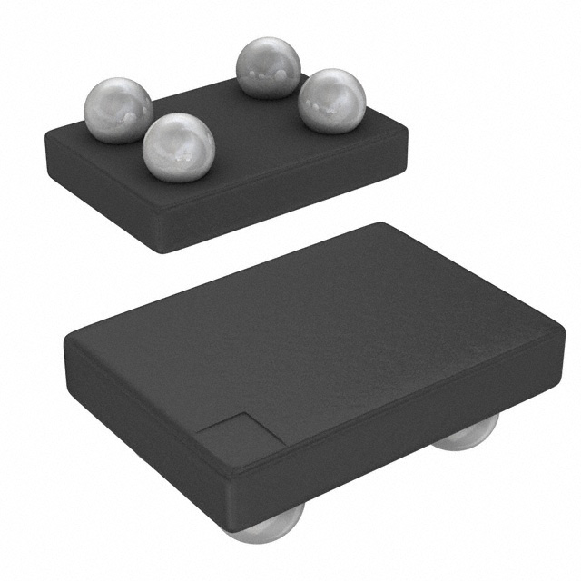
- Part No.:
- DS2502X1
- Manufacturer:
- Analog Devices Inc./Maxim Integrated
- Category:
- Memory
- Package:
- 4-UFBGA, WLCSP
- Datasheet:
-
 DS2502X1.pdf
- Description:
- IC EPROM 1KBIT 1-WIRE 4WLP
- Quantity:
- Payment:

- Shipping:

Inventory:4,339
Please send an inquiry. Send us your inquiry, and we will respond immediately.
Product details
Overview
DS2502X1 from Maxim Integrated is a 1-Wire add-only memory IC with factory-lasered 64-bit ROM ID, 1024-bit EPROM (4 × 256-bit pages), page-level write protection, and parasitic power operation. It serves as a tamper-resistant traceability tag for calibration data, asset tracking, and maintenance records in industrial and embedded systems.
For engineers reviewing the DS2502X1 datasheet, DS2502X1 pinout, DS2502X1 application, or DS2502X1 equivalent, this device requires 12V programming pulses, supports 16.3kbps 1-Wire communication, operates from 2.8V–6.0V at –40°C to +85°C, and uses a single DATA/GND interface - critical for space-constrained, low-pin-count designs.
Technical Context
The DS2502X1 implements a hierarchical 1-Wire protocol: ROM function commands (e.g., Read ROM, Skip ROM) must be executed first to access memory functions. Its internal architecture includes an 8-bit scratchpad buffer, on-chip 8-bit CRC generator, and program-voltage detection circuitry that triggers only during 12V pulses.
EPROM programming follows a strict bit-wise 1→0 transition rule; no bit can be reset from 0 to 1. Page Address Redirection Bytes (in Status Memory) enable software-level data patching by mapping invalid pages to replacement pages - a key enabler for field-updatable calibration or revision data without physical replacement.
Key Specifications
| Parameter | Value and Actual Design Meaning |
|---|---|
| Memory Type | 1024-bit EPROM (4 pages × 32 bytes), plus 64-bit lasered ROM and 64-bit status memory |
| Interface | Single-pin 1-Wire bus with parasitic power - eliminates dedicated VCC and simplifies PCB routing |
| Programming Voltage | 11.5V–12.0V pulse (480 µs duration); required only during EPROM write - not needed for read or ROM access |
| Operating Voltage | 2.8V–6.0V for reads; full functionality across –40°C to +85°C industrial temperature range |
| Data Integrity | On-the-fly 8-bit CRC generation per page during Read Data/Generate CRC command - ensures real-time validity of dynamic content |
| Write Protection | Per-page permanent write lock via Status Byte bits - prevents accidental or malicious overwrites after commissioning |
| Family Code | 09h (hex) - identifies device class to 1-Wire master and enables automatic protocol selection |
Pinout & Package
DS2502X1 is packaged in a 4-terminal Wafer-Level Package (WLP), qualified for surface-mount assembly. Pin 1 = DATA (bidirectional 1-Wire I/O), Pins 2A/2B = GND (dual ground terminals for robust return path), and "rrd" laser mark indicates revision/date code. No NC or VCC pins - power derived entirely from DATA line.
| Pin/Terminal | Circuit Role | Design Meaning |
|---|---|---|
| 1 (DATA) | 1-Wire bidirectional I/O | Carries all protocol signals (presence detect, ROM commands, memory reads/writes) and powers device parasitically |
| 2A (GND) | Ground reference | Primary return path for 1-Wire signaling and programming current - low-impedance connection essential for CRC accuracy |
| 2B (GND) | Ground reference | Secondary ground terminal - improves noise immunity and thermal dissipation in high-reliability deployments |
Key Features
| Feature | Design Value |
|---|---|
| Add-only memory architecture | Enables field updates by appending new data without erasing prior content - ideal for maintenance logs and firmware version history |
| Page Address Redirection | Allows software to invalidate obsolete pages and redirect reads to updated pages - eliminates need for full-device reprogramming |
| Factory-lasered 64-bit ROM ID | Guarantees globally unique identity (8-bit family code + 48-bit serial + 8-bit CRC) - foundational for secure device authentication |
| Per-page write protection | Locks individual 256-bit pages permanently after programming - prevents tampering with calibration constants or security keys |
| Parasitic power operation | Eliminates external power supply and decoupling capacitors - reduces BOM count and board area in sensor nodes and legacy retrofits |
Applications
| Calibration Data Storage | Asset Tracking Tag |
|---|---|
|
Use Scenario: Storing factory-calibrated sensor offsets and gain coefficients in medical diagnostic equipment. IC Role / Device Role / Timing Role: Nonvolatile, tamper-proof memory node providing authenticated calibration data on demand via 1-Wire. Use Value: Ensures measurement traceability to NIST standards; write-protection prevents unauthorized drift correction. |
Use Scenario: Attaching to industrial tools or test fixtures to log usage cycles, maintenance dates, and operator IDs. IC Role / Device Role / Timing Role: Serialized identity anchor with append-only memory for lifetime service history. Use Value: Enables automated audit trails without battery or complex interface - compatible with handheld 1-Wire readers. |
| Firmware Revision Registry | Access Control Credential |
|
Use Scenario: Embedding in edge gateway modules to record bootloader version, secure boot state, and update timestamps. IC Role / Device Role / Timing Role: Immutable revision ledger supporting secure firmware rollback prevention. Use Value: Page redirection allows safe patching of revision metadata without risking corruption of active firmware image. |
Use Scenario: Integrating into smart locks or access panels to store encrypted credential seeds and revocation flags. IC Role / Device Role / Timing Role: Physically unclonable identity token with write-protected access policy storage. Use Value: Factory-lasered ROM ID provides hardware-rooted trust; status bytes flag compromised credentials without exposing keys. |
Equivalent & Alternatives
The following parts are listed as comparable options for similar add-only memory applications.
| Alternative Part | Technical Difference | Application Difference | Selection Advice |
|---|---|---|---|
| DS2430A | 256-bit EEPROM (not EPROM); supports byte-level erase/write; no page redirection; 5V-only operation | Limited to short-term configuration storage; lacks guaranteed uniqueness and permanent write lock | Choose DS2430A only if frequent rewrites are required and traceability is secondary. |
| DS28EC20 | 20kb EEPROM with SHA-256 crypto engine; 1-Wire interface; 1.8V–5.25V; no parasitic power support | Requires external VCC; adds cryptographic authentication but increases system complexity and cost | Select DS28EC20 when cryptographic integrity verification is mandatory and board space allows dual-supply design. |
Compared with DS2502X1, DS2430A offers rewrite flexibility but sacrifices absolute traceability and permanent protection, while DS28EC20 delivers cryptographic assurance at the cost of parasitic power capability and higher integration overhead - making DS2502X1 optimal for cost-sensitive, battery-free, high-integrity logging.
Availability
DS2502X1 is available at Aetrix Electronics and suitable for calibration data storage, asset tracking, firmware revision registry, and access control credential applications requiring stable component supply and long-term industrial lifecycle support.
Supply support for DS2502X1 includes scheduled delivery planning, volume procurement assistance, BOM continuity management, traceable sourcing, and lifecycle availability coordination for OEM customers, industrial embedded developers, connected-device designers, and electronics production programs.
Manufacturer
Maxim Integrated (now part of Analog Devices) designs precision analog, mixed-signal, and digital ICs for industrial, automotive, and communications markets - emphasizing reliability, integration, and low-power operation.
The DS2502X1 belongs to Maxim's 1-Wire memory product line, engineered specifically for secure, minimal-footprint device identification and immutable data logging in resource-constrained environments.
FAQ
What is the primary function of the DS2502X1 in a system?
The DS2502X1 serves as a secure, add-only memory node with guaranteed unique identity. It stores calibration data, asset history, or firmware metadata using its 1024-bit EPROM and factory-lasered 64-bit ROM ID. Its 1-Wire interface enables direct microcontroller connection with no external power - making DS2502X1 ideal for retrofitting legacy equipment or embedding in space-constrained sensors.
How does the DS2502X1 achieve tamper resistance?
The DS2502X1 achieves tamper resistance through three mechanisms: (1) permanent per-page write protection bits in status memory, (2) irreversible 1→0 bit programming - preventing restoration of erased data, and (3) factory-lasered 64-bit ROM ID with embedded CRC, which cannot be altered post-manufacture. These features ensure DS2502X1 remains a trusted source for calibration constants and access credentials even in unsecured physical environments.
Can the DS2502X1 be reprogrammed multiple times?
Yes, the DS2502X1 supports multiple programming cycles - but only in add-only mode: new data can be written to unused bits (1→0 transitions), and obsolete pages can be logically invalidated using Page Address Redirection Bytes. However, once a bit is programmed to '0', it cannot revert to '1'. So DS2502X1 is not rewritable like EEPROM, but its redirection architecture enables effective field updates without physical replacement.
What voltage and timing requirements apply to DS2502X1 programming?
DS2502X1 requires a precise 11.5V–12.0V programming pulse lasting 480 µs on the DATA line - delivered after successful CRC validation of the write command. This high-voltage pulse is generated externally by the bus master; reads operate at standard 2.8V–6.0V levels. The DS2502X1's internal voltage-detect circuit confirms pulse presence before enabling EPROM programming - ensuring DS2502X1 only commits data when conditions meet specification.
Is the DS2502X1 compatible with standard 1-Wire microcontroller libraries?
Yes, the DS2502X1 fully complies with the standard 1-Wire protocol stack: it responds to ROM Function Commands (Read ROM, Skip ROM) and supports Memory Function Commands (Read Memory, Write Memory, Read Status, etc.) with LSB-first bit ordering and built-in 8-bit CRC. Standard Maxim/Analog Devices 1-Wire drivers - including those for Arduino, STM32, and PIC - natively support DS2502X1 without modification, provided the host can generate the required 12V programming pulse.
DS2502X1 Specifications
- Product attributes
- Attribute value
- Manufacturer:
- Analog Devices Inc./Maxim Integrated
- Series:
- -
- Package/Case:
- 4-UFBGA, WLCSP
- Packaging:
- Tape & Reel (TR)
- Product Status:
- Obsolete
- Programmable:
- Not Verified
- Memory Type:
- Non-Volatile
- Memory Format:
- EPROM
- Technology:
- EPROM - OTP
- Memory Size:
- 1Kbit
- Memory Organization:
- 128 x 8
- Memory Interface:
- 1-Wire®
- Clock Frequency:
- -
- Write Cycle Time - Word, Page:
- -
- Access Time:
- -
- Voltage - Supply:
- 2.8V ~ 6V
- Operating Temperature:
- -40°C ~ 85°C (TA)
- Grade:
- -
- Qualification:
- -
- Mounting Type:
- Surface Mount
- Supplier Device Package:
- 4-WLP (1.62x0.93)
DS2502X1 FAQ
1.How can I place an order for DS2502X1 through Aetrix?
Please submit a Request for Quotation (RFQ) for DS2502X1 on Aetrix. Our sales agent will provide a competitive quotation and guide you through the order confirmation once you accept the terms.
2.Are the price and stock information for DS2502X1 reliable?
The price and inventory of DS2502X1 are updated periodically and may fluctuate due to market conditions. Stock and pricing data are typically refreshed every 24 hours. Quotation validity for DS2502X1 is usually 5 days.
3.What payment methods are accepted for DS2502X1?
We accept Wire Transfer, PayPal, Credit Card, Western Union, MoneyGram, and Escrow for DS2502X1 transactions.
Note: Certain payment methods may incur a processing fee.
4.How is shipping managed for DS2502X1?
DS2502X1 orders can be shipped via leading logistics carriers, including DHL, UPS, FedEx, TNT, or Registered Mail.
Once your DS2502X1 order is processed, you will receive an email with the shipment details and tracking number.
Note: Tracking information may take up to 24 hours to appear. Express delivery typically takes 3–5 business days.
5.How can I obtain technical support or documentation for DS2502X1?
For technical support, including DS2502X1 datasheets, pinout diagrams, or application guidance, please contact our engineering support team. They can provide detailed documentation and assistance for your DS2502X1 requirements.
6.How does Aetrix verify that DS2502X1 is sourced from the original manufacturer or authorized distributors?
All DS2502X1 products on Aetrix are procured from qualified distributors and authorized channels. Our dedicated quality assurance team conducts strict verification, including traceability checks and, if necessary, third-party testing. This ensures that DS2502X1 meets industry standards.
7.What is the process for return or replacement of DS2502X1?
All DS2502X1 units undergo pre-shipment inspection (PSI). If there is an issue with DS2502X1, returns or replacements are accepted under the following conditions:
1.Quantity discrepancies, incorrect items, or visible external defects (such as breakage or corrosion), acknowledged by Aetrix.
2.The issue is reported within 90 days of delivery.
3.The DS2502X1 part is unused and in its original packaging.
Return procedure for DS2502X1:
1.Submit a request within 90 days.
2.Obtain a Return Material Authorization (RMA) from Aetrix.
DS2502X1 Tags

-
M24C02-WMN6TP
STMicroelectronics

-
AT24C02C-XHM-T
Microchip Technology

-
AT21CS01-STUM10-T
Microchip Technology

-
AT24C02C-SSHM-T
Microchip Technology

-
24LC01BT-I/OT
Microchip Technology

-
M24C02-FMC6TG
STMicroelectronics
-
AT24CS02-SSHM-T
Microchip Technology

-
93LC46BT-I/OT
Microchip Technology
-
AT24C04C-SSHM-T
Microchip Technology

-
24LC01BT-I/SN
Microchip Technology
-
24AA02UIDT-I/OT
Microchip Technology

-
AT24C08C-STUM-T
Microchip Technology
Tech Hub

Comparator circuit design covering voltage thresholds, input limits, open-collector outputs, LM393 wiring, op-amp differences, hysteresis, timing, window detection and practical fault diagnosis.

Schmitt triggers use separate rising and falling thresholds to stabilize slow or noisy signals. This guide covers hysteresis, 74HC14 and 74HCT14 selection, comparator calculations, RC oscillators and p…

Counterfeit components can hide behind convincing markings and passing basic function tests. This engineering reference covers source traceability, external inspection, X-ray, XRF, electrical testing, …

A practical engineering and sourcing framework covering lifecycle verification, lifetime-buy calculations, replacement qualification, supplier checks and counterfeit-risk controls.

TTL and CMOS logic families differ in thresholds, loading, output drive, power and timing. This engineering guide compares 74HC and 74HCT, calculates noise margins and checks 3.3 V/5 V compatibility.

A practical engineering guide to 3.3V and 5V logic compatibility, input thresholds, resistor dividers, translator ICs, MOSFET level shifting, I2C pull-ups, timing limits and power-sequencing risks.

The 74HC595 uses push-pull logic outputs, while the TPIC6B595 uses 50 V open-drain DMOS sinks for higher-power loads. This guide compares timing, current limits, 3.3 V interfacing, load wiring, thermal…

The 74HC595 converts serial data into eight stable parallel outputs. This guide covers pin functions, shift and storage timing, OE and MR behavior, drive-current limits, cascading, voltage compatibilit…

A technical comparison of level-sensitive latches and edge-triggered flip-flops, covering timing windows, setup and hold limits, master–slave operation, time borrowing, race-through, HDL inference and…

A D latch stores one bit while Enable controls when data can pass. This reference covers gate-level operation, truth tables, transparency, setup and hold timing, LE versus OE, common ICs and practical …


