
 My Inquiry
 My Account


Analog Devices Inc./Maxim Integrated DS28DG02G-3C+
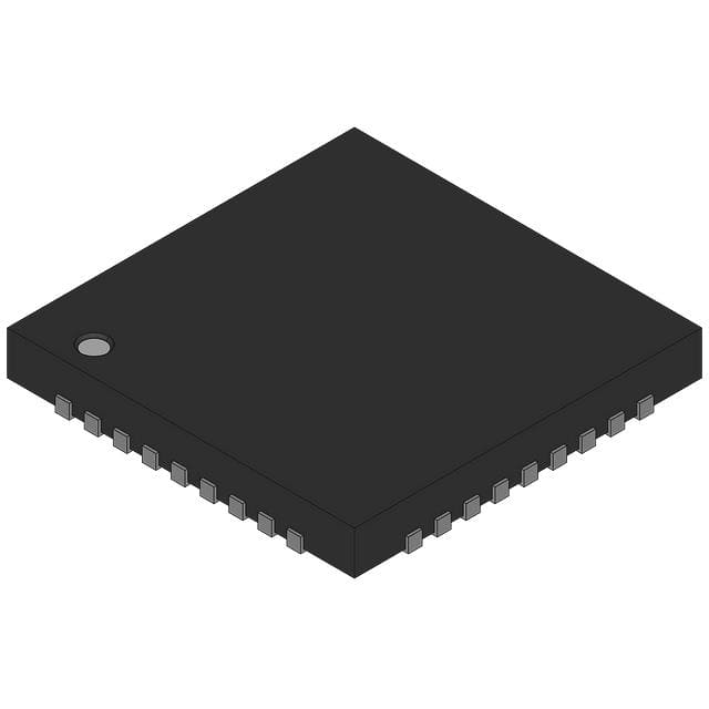
- Part No.:
- DS28DG02G-3C+
- Manufacturer:
- Analog Devices Inc./Maxim Integrated
- Category:
- Memory
- Package:
- 36-WFQFN Exposed Pad
- Datasheet:
-
 DS28DG02G-3C+.pdf
- Description:
- IC EEPROM 2KBIT SPI 2MHZ 36TQFN
- Quantity:
- Payment:

- Shipping:

Inventory:4,237
Please send an inquiry. Send us your inquiry, and we will respond immediately.
Product details
Overview
DS28DG02G-3C+ from Maxim Integrated is a 2Kb SPI EEPROM IC integrating 12 bidirectional PIOs, RTC/calendar with leap-year compensation, CPU reset monitor, battery monitor (2.5V/2.25V/2.0V/1.75V thresholds), and programmable watchdog timer (1.6s/0.8s/0.4s/0.2s). It operates from 2.2V to 5.25V across –40°C to +85°C and is used in asset-tracking systems and patient-monitoring devices where nonvolatile configuration, time-stamping, and system supervision are required.
For engineers reviewing the DS28DG02G-3C+ datasheet, DS28DG02G-3C+ pinout, DS28DG02G-3C+ application, or DS28DG02G-3C+ equivalent, key selection considerations include its 36-pin TQFN-EP (6mm × 6mm) package, SPI Mode (0,0)/(1,1) compatibility up to 2MHz, factory-set 3.3V –5% VCC trip point, user-programmable battery threshold and watchdog timeout, and BCD-format RTC with alarm granularity down to seconds.
Technical Context
The DS28DG02G-3C+ implements a unified SPI interface supporting both Mode (0,0) and Mode (1,1) at up to 2MHz, enabling direct integration with legacy and modern microcontrollers without protocol translation. Its RTC uses a 32.768kHz crystal or external TCXO input and maintains BCD-encoded time/date with automatic leap-year correction through year 2099.
Power supervision includes a precision VCC monitor with 0.5% hysteresis and debounce for manual reset, a separately configurable battery monitor with five selectable thresholds, and a watchdog timer whose timeout is stored in NV SRAM at address 134h. All 12 PIOs support push-pull or open-drain output type per group of four, with power-on state, direction, and read-inversion stored in nonvolatile EEPROM.
Key Specifications
| Parameter | Value and Actual Design Meaning |
|---|---|
| EEPROM Capacity | 2Kb (256 × 8), organized as four 64-byte blocks with single-byte and 16-byte page writes |
| SPI Interface | Supports Modes (0,0) and (1,1) up to 2MHz; enables interoperability with diverse host MCUs |
| RTC Accuracy | ±46ppm frequency deviation with 32.768kHz crystal (12.5pF, ESR ≤ 45kΩ) |
| VCC Monitor Trip | Factory-set at 3.3V –5% (2.97V min, 3.14V max); provides reliable CPU reset under brownout |
| Battery Monitor Thresholds | User-selectable: 2.5V, 2.25V, 2.0V, or 1.75V; supports backup-supply health monitoring |
| Watchdog Timeout | Programmable to 1.6s, 0.8s, 0.4s, or 0.2s (typ); ensures deterministic system recovery |
| Operating Range | 2.2V to 5.25V supply voltage; –40°C to +85°C ambient temperature |
Pinout & Package
DS28DG02G-3C+ is housed in a 36-lead, 6mm × 6mm exposed-pad TQFN package (PKG CODE T3666+3), requiring soldering of the EP pad to the PCB ground plane for thermal and electrical integrity.
| Pin/Terminal | Circuit Role | Design Meaning |
|---|---|---|
| X1 / X2 | Crystal oscillator inputs | Connect 32.768kHz crystal (12.5pF) or TCXO output; enable RTC timing source |
| RSTZ | Open-drain reset output / manual reset input | Active-low CPU reset triggered by VCC dropout, watchdog alarm, or pushbutton; debounced |
| WDI | Watchdog input | Active-high feed signal; failure to toggle within timeout asserts WDOZ/ALMZ |
| WDOZ | Open-drain watchdog alarm output | Configurable active-low alarm output for watchdog timeout events |
| WPZ | Hardware write-protect input | Active-low pin enabling block-level EEPROM write protection (1/2/all blocks) |
| PIO0–PIO11 | Programmable I/O lines | 12 bidirectional pins configurable as input/output, push-pull/open-drain, with NV power-on defaults |
| VBAT | Backup battery supply | Powers RTC and RSTZ during main supply loss; supports battery health monitoring |
| ALMZ | Open-drain alarm output | Active-low output for RTC alarm, battery monitor alarm, or user-selected watchdog alarm |
| SO/SI/SCK/CSZ | SPI serial interface | Standard 4-wire SPI bus (MISO/MOSI/SCLK/SS) for EEPROM, register, and configuration access |
Key Features
| Feature | Design Value |
|---|---|
| Unique 64-bit registration number | Factory-programmed ROM ID at addresses 118h–11Fh; enables device-level traceability and secure identification |
| EEPROM endurance & retention | 200k write cycles per page at +25°C; 40-year data retention at +85°C - suitable for long-life industrial logging |
| PIO flexibility | Each of 12 PIOs independently configurable as input/output; output type (push-pull/open-drain) set per group of 4; power-on state stored in NV memory |
| RTC/calendar alarm granularity | Alarm configurable to trigger every second, minute, hour, day, week, or month - supports precise event scheduling |
| ESD robustness | ±4kV IEC 1000-4-2 level on all pins except X1/X2 - enhances field reliability in noisy environments |
Applications
| Asset-Tracking Systems | Patient-Monitoring Systems |
|---|---|
Use Scenario: Tamper-evident, time-stamped location logging in portable medical asset tags. IC Role / Device Role / Timing Role: DS28DG02G-3C+ stores unique device ID, calibration data, and timestamped GPS coordinates using its 2Kb EEPROM and RTC. Use Value: Enables audit-compliant chain-of-custody records with BCD calendar accuracy and leap-year correction through 2099. | Use Scenario: Battery-backed vital-sign recorder with low-power sleep and periodic wake-up for sensor sampling. IC Role / Device Role / Timing Role: DS28DG02G-3C+ supplies real-time timestamps, monitors battery health (VBAT), and triggers watchdog reset if firmware hangs. Use Value: Ensures clinical data integrity via nonvolatile RTC and 2.25V–2.5V battery threshold detection with ±2.5% tolerance. |
| Home Lighting Control Systems | Holter Heart Monitors |
Use Scenario: Smart switch module with scheduled on/off control and energy usage logging. IC Role / Device Role / Timing Role: DS28DG02G-3C+ executes RTC-based scheduling, stores user preferences in EEPROM, and drives status LEDs via PIO outputs. Use Value: Delivers LED drive capability (up to 30mA sink at 5.25V) and push-pull/open-drain configurability for direct indicator control. | Use Scenario: Wearable cardiac monitor with multi-day continuous ECG recording and timestamped anomaly detection. IC Role / Device Role / Timing Role: DS28DG02G-3C+ provides accurate time-of-event stamping, manages backup power via VBAT, and asserts ALMZ on battery low condition. Use Value: Guarantees 40-year EEPROM data retention at +85°C - critical for long-term diagnostic data archival compliance. |
Equivalent & Alternatives
The following parts are listed as comparable options for similar multifunction supervisory EEPROM applications.
| Alternative Part | Technical Difference | Application Difference | Selection Advice |
|---|---|---|---|
| DS28E02-3C+ | 2Kb SPI EEPROM only; no RTC, PIO, watchdog, or voltage monitors | Limited to pure nonvolatile storage; lacks timekeeping, I/O, and system supervision | Select when only EEPROM functionality is needed and board space/power budget preclude integrated peripherals |
| MAX31329E–3C+ | Standalone RTC with I²C interface; no EEPROM, PIO, or supervision features | Provides higher-accuracy RTC (±5ppm) but requires separate EEPROM and reset IC for full DS28DG02G-3C+ functionality | Select when ultra-precise timekeeping is primary requirement and system architecture favors discrete functions |
Compared with DS28DG02G-3C+, DS28E02-3C+ reduces integration but simplifies design for storage-only use, while MAX31329E–3C+ improves RTC accuracy at the cost of increased component count and loss of unified SPI control.
Availability
DS28DG02G-3C+ is available at Aetrix Electronics and suitable for asset-tracking systems, patient-monitoring systems, home lighting control systems, and Holter heart monitors requiring stable component supply, long-term data retention, and integrated timekeeping with system supervision.
Supply support for DS28DG02G-3C+ includes scheduled delivery planning, volume procurement assistance, BOM continuity management, traceable sourcing, and lifecycle availability coordination for OEM customers, industrial embedded developers, connected-device designers, and electronics production programs.
Manufacturer
Maxim Integrated (now part of Analog Devices) designs precision analog, mixed-signal, and digital ICs for industrial, medical, and communications applications.
The DS28DG02G-3C+ belongs to Maxim's multifunction supervisory EEPROM product line, engineered to consolidate EEPROM, RTC, GPIO, reset, battery monitoring, and watchdog functions into a single SPI-accessible device for space-constrained, battery-aware embedded systems.
FAQ
What is the package type and thermal requirement for DS28DG02G-3C+
The DS28DG02G-3C+ uses a 36-lead TQFN-EP package (6mm × 6mm) with an exposed paddle. The EP pad must be soldered to the PCB ground plane to ensure proper thermal dissipation and electrical performance, as specified in Maxim Application Note 3273. This is mandatory for reliable operation across the full –40°C to +85°C range.
How does the DS28DG02G-3C+ RTC handle leap years?
The DS28DG02G-3C+ RTC automatically compensates for leap years by adding February 29 in any year divisible by 4, including year 2000, and correctly excludes year 2100. This logic is hardwired and operates continuously in BCD format, ensuring calendar accuracy through year 2099 without host intervention or software updates.
Can DS28DG02G-3C+ operate without a backup battery connected to VBAT?
Yes - DS28DG02G-3C+ can operate without a VBAT connection; in that case, VBAT must be tied to VCC. However, RTC and RSTZ functionality will be lost during VCC power loss, and the battery monitor feature becomes inactive. The device continues full EEPROM, PIO, and watchdog operation powered solely by VCC.
What are the valid SPI clock frequencies and modes supported by DS28DG02G-3C+
The DS28DG02G-3C+ supports SPI Modes (0,0) and (1,1) with a maximum clock frequency of 2MHz. Timing parameters including tDS (50ns), tDH (50ns), and tV (120ns max) are guaranteed over the full operating range. Mode selection is automatic based on SCK/CSZ phase relationship - no configuration register setting is required.
How is write protection implemented on DS28DG02G-3C+ EEPROM blocks?
DS28DG02G-3C+ EEPROM write protection is controlled via the WPZ pin and internal registers. Hardware protection is enabled by pulling WPZ low; software control allows selective protection of block 3 only, blocks 2–3, or all four 64-byte blocks. Protection applies to both user EEPROM (000h–0FFh) and NV registers ≥120h, preventing accidental overwrite during system operation.
DS28DG02G-3C+ Specifications
- Product attributes
- Attribute value
- Manufacturer:
- Analog Devices Inc./Maxim Integrated
- Series:
- -
- Package/Case:
- 36-WFQFN Exposed Pad
- Packaging:
- Tube
- Product Status:
- Obsolete
- Programmable:
- Not Verified
- Memory Type:
- Non-Volatile
- Memory Format:
- EEPROM
- Technology:
- EEPROM
- Memory Size:
- 2Kbit
- Memory Organization:
- 256 x 8
- Memory Interface:
- SPI
- Clock Frequency:
- 2 MHz
- Write Cycle Time - Word, Page:
- -
- Access Time:
- -
- Voltage - Supply:
- 2.2V ~ 5.25V
- Operating Temperature:
- -40°C ~ 85°C (TA)
- Grade:
- -
- Qualification:
- -
- Mounting Type:
- Surface Mount
- Supplier Device Package:
- 36-TQFN (6x6)
DS28DG02G-3C+ FAQ
1.How can I place an order for DS28DG02G-3C+ through Aetrix?
Please submit a Request for Quotation (RFQ) for DS28DG02G-3C+ on Aetrix. Our sales agent will provide a competitive quotation and guide you through the order confirmation once you accept the terms.
2.Are the price and stock information for DS28DG02G-3C+ reliable?
The price and inventory of DS28DG02G-3C+ are updated periodically and may fluctuate due to market conditions. Stock and pricing data are typically refreshed every 24 hours. Quotation validity for DS28DG02G-3C+ is usually 5 days.
3.What payment methods are accepted for DS28DG02G-3C+?
We accept Wire Transfer, PayPal, Credit Card, Western Union, MoneyGram, and Escrow for DS28DG02G-3C+ transactions.
Note: Certain payment methods may incur a processing fee.
4.How is shipping managed for DS28DG02G-3C+?
DS28DG02G-3C+ orders can be shipped via leading logistics carriers, including DHL, UPS, FedEx, TNT, or Registered Mail.
Once your DS28DG02G-3C+ order is processed, you will receive an email with the shipment details and tracking number.
Note: Tracking information may take up to 24 hours to appear. Express delivery typically takes 3–5 business days.
5.How can I obtain technical support or documentation for DS28DG02G-3C+?
For technical support, including DS28DG02G-3C+ datasheets, pinout diagrams, or application guidance, please contact our engineering support team. They can provide detailed documentation and assistance for your DS28DG02G-3C+ requirements.
6.How does Aetrix verify that DS28DG02G-3C+ is sourced from the original manufacturer or authorized distributors?
All DS28DG02G-3C+ products on Aetrix are procured from qualified distributors and authorized channels. Our dedicated quality assurance team conducts strict verification, including traceability checks and, if necessary, third-party testing. This ensures that DS28DG02G-3C+ meets industry standards.
7.What is the process for return or replacement of DS28DG02G-3C+?
All DS28DG02G-3C+ units undergo pre-shipment inspection (PSI). If there is an issue with DS28DG02G-3C+, returns or replacements are accepted under the following conditions:
1.Quantity discrepancies, incorrect items, or visible external defects (such as breakage or corrosion), acknowledged by Aetrix.
2.The issue is reported within 90 days of delivery.
3.The DS28DG02G-3C+ part is unused and in its original packaging.
Return procedure for DS28DG02G-3C+:
1.Submit a request within 90 days.
2.Obtain a Return Material Authorization (RMA) from Aetrix.
DS28DG02G-3C+ Tags

-
M24C02-WMN6TP
STMicroelectronics

-
AT24C02C-XHM-T
Microchip Technology

-
AT21CS01-STUM10-T
Microchip Technology

-
AT24C02C-SSHM-T
Microchip Technology

-
24LC01BT-I/OT
Microchip Technology

-
M24C02-FMC6TG
STMicroelectronics
-
AT24CS02-SSHM-T
Microchip Technology

-
93LC46BT-I/OT
Microchip Technology
-
AT24C04C-SSHM-T
Microchip Technology

-
24LC01BT-I/SN
Microchip Technology
-
24AA02UIDT-I/OT
Microchip Technology

-
AT24C08C-STUM-T
Microchip Technology
Tech Hub

Comparator circuit design covering voltage thresholds, input limits, open-collector outputs, LM393 wiring, op-amp differences, hysteresis, timing, window detection and practical fault diagnosis.

Schmitt triggers use separate rising and falling thresholds to stabilize slow or noisy signals. This guide covers hysteresis, 74HC14 and 74HCT14 selection, comparator calculations, RC oscillators and p…

Counterfeit components can hide behind convincing markings and passing basic function tests. This engineering reference covers source traceability, external inspection, X-ray, XRF, electrical testing, …

A practical engineering and sourcing framework covering lifecycle verification, lifetime-buy calculations, replacement qualification, supplier checks and counterfeit-risk controls.

TTL and CMOS logic families differ in thresholds, loading, output drive, power and timing. This engineering guide compares 74HC and 74HCT, calculates noise margins and checks 3.3 V/5 V compatibility.

A practical engineering guide to 3.3V and 5V logic compatibility, input thresholds, resistor dividers, translator ICs, MOSFET level shifting, I2C pull-ups, timing limits and power-sequencing risks.

The 74HC595 uses push-pull logic outputs, while the TPIC6B595 uses 50 V open-drain DMOS sinks for higher-power loads. This guide compares timing, current limits, 3.3 V interfacing, load wiring, thermal…

The 74HC595 converts serial data into eight stable parallel outputs. This guide covers pin functions, shift and storage timing, OE and MR behavior, drive-current limits, cascading, voltage compatibilit…

A technical comparison of level-sensitive latches and edge-triggered flip-flops, covering timing windows, setup and hold limits, master–slave operation, time borrowing, race-through, HDL inference and…

A D latch stores one bit while Enable controls when data can pass. This reference covers gate-level operation, truth tables, transparency, setup and hold timing, LE versus OE, common ICs and practical …


