
 My Inquiry
 My Account


STMicroelectronics DSM2180F3-90T6
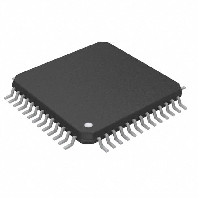
- Part No.:
- DSM2180F3-90T6
- Manufacturer:
- STMicroelectronics
- Category:
- Memory
- Package:
- 52-QFP
- Datasheet:
-
 DSM2180F3-90T6.pdf
- Description:
- IC FLASH 1MBIT PARALLEL 52PQFP
- Quantity:
- Payment:

- Shipping:

Inventory:1,173
Please send an inquiry. Send us your inquiry, and we will respond immediately.
Product details
Overview
DSM2180F3-90T6 from Lattice Semiconductor is a programmable DSP system memory device designed for seamless integration with Analog Devices ADSP-218X family DSPs. It integrates 128 KB (128K × 8) Flash memory, a 3,000-gate CPLD with 16 macrocells, up to 16 configurable I/O pins, and JTAG in-system programming - all operating at 5 V ±10% with 90 ns access time in PQFP52 package. It enables glueless bootloading via Byte DMA and external data overlay memory access for firmware updates in battery-powered embedded audio or telecom signal processing systems.
For engineers reviewing the DSM2180F3-90T6 datasheet, DSM2180F3-90T6 pinout, DSM2180F3-90T6 application, or DSM2180F3-90T6 equivalent, key selection criteria include BDMA vs. DMS memory access modes, sector-protected Flash erasability (100K cycles), PLD runtime macrocell register accessibility via DSP data bus, and zero-power standby current (75 µA) for low-power DSP co-processor designs.
Technical Context
The DSM2180F3-90T6 implements a dual-mode memory interface: Byte DMA (BMS strobe) for high-speed boot code loading and Data Memory Overlay (DMS strobe) for byte-wise Flash programming without BDMA channel reinitialization. Its Decode PLD (DPLD) dynamically maps eight 16 KB Flash sectors across the ADSP-218X address space using an 8-bit Page Register updated in real time.
Its Complex PLD (CPLD) contains 16 input macrocells (IMCs) for debounced I/O sampling and 16 output macrocells (OMCs) directly connected to the DSP data bus - enabling real-time read/write of shifter/counter state registers. Both PLDs support Turbo/Non-Turbo mode switching via runtime control registers to balance propagation delay (<15 ns combinatorial) and power consumption.
Key Specifications
| Parameter | Value and Actual Design Meaning |
|---|---|
| Flash Memory | 128 KB (128K × 8), organized as eight 16 KB erasable sectors matching ADSP-218X overlay window size for direct firmware partitioning. |
| Access Time | 90 ns maximum - defines minimum DSP wait-state insertion for reliable BDMA/DMS read cycles at full 5V operation. |
| PLD Capacity | 3,000 usable gates with 16 macrocells - sufficient for UART chip selects, keypad scan logic, or LCD timing generators without external glue logic. |
| I/O Pins | Up to 16 multifunction pins (Ports B/C/D), software- or PLD-controllable with 8 mA drive strength at 5 V for direct LED/display interfacing. |
| Power Consumption | 75 µA standby current - achieved via automatic zero-power mode between memory accesses or PLD input transitions. |
| JTAG ISP | Full-chip programming in 10–20 seconds without DSP involvement - enables JIT inventory, field firmware updates, and secure blank-board manufacturing. |
| Security | Programmable security bit blocks JTAG access to Flash and PLD configuration; DSP retains full read access to Flash contents. |
Pinout & Package
DSM2180F3-90T6 is housed in a 52-pin Plastic Quad Flatpack (PQFP52) package with 0.65 mm lead pitch, compliant with JEDEC MS-026. Thermal resistance θJA = 45°C/W supports operation up to +70°C ambient in compact DSP carrier boards.
| Pin/Terminal | Circuit Role | Design Meaning |
|---|---|---|
| AD0–AD7 | DSP Data Bus (Lower Byte) | 8-bit bidirectional interface for BDMA reads, DMS writes, and csiop register access - matches ADSP-218X byte-wide data path. |
| AD8–AD15 | DSP Address Bus (Upper Byte) | Provides A8–A15 for Flash sector decoding and PLD address mapping; used with Page Register to select 16 KB overlay windows. |
| BMS, DMS, IOMS | DSP Memory Strobes | BMS enables Byte DMA Flash reads; DMS enables overlay memory writes; IOMS accesses 256-byte csiop control register block. |
| PD0–PD2 | Chip Select Inputs | PD2 = CSI (PSD Chip Select Input); PD0/PD1 optionally routed to DPLD for external peripheral chip selects (e.g., UART, codec). |
| PA0–PA7 | DSP Address Bus (Lower Byte) | A0–A7 used by DPLD for fine-grained sector addressing within selected 16 KB window; required for Flash program/erase sequencing. |
| PB0–PB7, PC0–PC7 | Configurable I/O Ports | 16 pins total; each individually assignable as input, output, or PLD-controlled - supports keypad matrix scanning or LCD data lines. |
| TCK, TMS, TDI, TDO | JTAG ISP Interface | IEEE 1149.1-compliant boundary-scan port for in-circuit Flash/PLD programming and security bit configuration. |
Key Features
| Feature | Design Value |
|---|---|
| Glueless DSP Interface | Direct connection to ADSP-218X address/data/control signals eliminates level shifters, buffers, or address latches in two-chip system designs. |
| Dual-Mode Flash Access | Supports both BDMA (for fast bootloading) and DMS-based overlay writes (for efficient firmware patching without DMA setup overhead). |
| Runtime PLD Control | 16 OMCs accessible as memory-mapped registers via csiop - allows DSP to dynamically reconfigure counters, state machines, or clock dividers. |
| Sector-Level Flash Protection | Individual 16 KB sector lock bits prevent accidental erase/write - critical for preserving bootloader code while updating application firmware. |
| Zero-Power Standby | Automatic transition to 75 µA quiescent current when idle - extends battery life in portable DSP-based voice recorders or sensor nodes. |
Applications
| Telecom Voice Processing | Industrial Motor Control |
|---|---|
|
Use Scenario: Real-time echo cancellation and DTMF detection in VoIP gateways using ADSP-2185. IC Role / Device Role / Timing Role: DSM2180F3-90T6 serves as boot ROM and overlay memory for algorithm coefficients, with PLD generating UART control signals and interrupt flags. Use Value: 90 ns Flash access enables sub-100 µs coefficient load times; sector protection isolates boot code from field-updated filter tables. |
Use Scenario: Closed-loop servo positioning in CNC controllers using ADSP-2186. IC Role / Device Role / Timing Role: DSM2180F3-90T6 stores motor profile lookup tables and implements encoder quadrature decoding logic in CPLD. Use Value: Direct DSP read/write of OMC registers allows real-time adjustment of position error thresholds without PLD recompilation. |
| Portable Audio Recorders | Medical Signal Analyzers |
|
Use Scenario: Battery-powered digital voice recorder with ADSP-2181 handling MP3 encoding. IC Role / Device Role / Timing Role: DSM2180F3-90T6 provides boot code storage, overlay memory for encoder buffers, and drives OLED display via Port B. Use Value: 75 µA standby current extends runtime between charges; JTAG ISP enables factory programming of region-specific firmware variants. |
Use Scenario: Portable ECG analyzer using ADSP-2184 for real-time QRS detection. IC Role / Device Role / Timing Role: DSM2180F3-90T6 holds clinical algorithm libraries and implements SPI master logic for ADC data acquisition. Use Value: Security bit prevents unauthorized extraction of proprietary diagnostic IP; 100K Flash erase cycles support >5-year device lifespan. |
Equivalent & Alternatives
The following parts are listed as comparable options for similar DSP system memory applications.
| Alternative Part | Technical Difference | Application Difference | Selection Advice |
|---|---|---|---|
| DSM2180F3-70T6 | 70 ns access time (vs. 90 ns); identical Flash/PLD/I/O specs and pinout. | Required for ADSP-218X systems running at >20 MHz where tighter timing margins demand faster memory. | Select only if DSP clock frequency exceeds 20 MHz and timing analysis confirms need for reduced access latency. |
| DSM2181F3-90T6 | Adds 2 KB SRAM (vs. none); same Flash/PLD/I/O but different csiop register map and Page Register behavior. | Suitable when DSP requires small on-device scratchpad RAM alongside overlay memory - e.g., for real-time FFT buffer staging. | Choose only if application needs dedicated SRAM not provided by ADSP-218X internal memory or external SDRAM. |
Compared with DSM2180F3-90T6, the -70T6 variant reduces memory access latency for higher-clock DSPs but offers no functional extension, while the DSM2181F3-90T6 adds SRAM at the cost of register compatibility - making the -90T6 optimal for pure Flash-overlay+PLD expansion in cost- and power-sensitive ADSP-218X designs.
Availability
DSM2180F3-90T6 is available at Aetrix Electronics and suitable for telecom voice processing, industrial motor control, portable audio recorders, and medical signal analyzers requiring stable component supply across multi-year production cycles.
Supply support for DSM2180F3-90T6 includes scheduled delivery planning, volume procurement assistance, BOM continuity management, traceable sourcing, and lifecycle availability coordination for OEM customers, industrial embedded developers, connected-device designers, and electronics production programs.
Manufacturer
Lattice Semiconductor is a fabless provider of programmable logic devices, specializing in low-power FPGA, CPLD, and system memory solutions for embedded control and signal processing.
The DSM (Digital Signal Processor System Memory) product line targets ADSP-218X users needing integrated Flash, PLD, and I/O in a single chip - reducing board area, EMI, and power versus discrete memory + PLD implementations.
FAQ
What is the role of the Page Register in DSM2180F3-90T6 operation?
The 8-bit Page Register is a runtime-accessible csiop control register that directly feeds address translation logic in both the Decode PLD and Complex PLD. It determines which of the eight 16 KB Flash sectors is mapped into the current DSP external data overlay window, enabling dynamic firmware partitioning without hardware address decoding changes.
Can the PLD logic be modified after the device is soldered to the PCB?
Yes - the CPLD and DPLD configuration is stored in Flash memory and reprogrammable via JTAG ISP at any time, even in the final assembled product. No socket or UV erasure is needed; programming takes 10–20 seconds using a FlashLINK™ cable connected to a standard PC parallel port.
How does the security bit affect DSP access to Flash memory?
When the security bit is set, JTAG programmers cannot read or write Flash or PLD configuration, but the ADSP-218X DSP retains full read access to Flash contents through its AD0–AD7 data bus. This allows secure field deployment of boot code while permitting runtime execution and overlay data reads.
What is the difference between BDMA and DMS access modes for Flash memory?
BDMA (Byte DMA) uses the BMS strobe for high-speed sequential Flash reads during bootloading, but requires full channel setup per byte for writes. DMS (Data Memory Overlay) uses the DMS strobe to treat Flash as standard external RAM - enabling simpler, faster byte-wise writes without DMA overhead, though only the upper byte of each 16-bit DSP word is written.
DSM2180F3-90T6 Specifications
- Product attributes
- Attribute value
- Manufacturer:
- STMicroelectronics
- Series:
- -
- Package/Case:
- 52-QFP
- Packaging:
- Tray
- Product Status:
- Obsolete
- Programmable:
- Not Verified
- Memory Type:
- Non-Volatile
- Memory Format:
- FLASH
- Technology:
- FLASH
- Memory Size:
- 1Mbit
- Memory Organization:
- 128K x 8
- Memory Interface:
- Parallel
- Clock Frequency:
- -
- Write Cycle Time - Word, Page:
- -
- Access Time:
- 90 ns
- Voltage - Supply:
- 4.5V ~ 5.5V
- Operating Temperature:
- -40°C ~ 85°C (TA)
- Grade:
- -
- Qualification:
- -
- Mounting Type:
- Surface Mount
- Supplier Device Package:
- 52-PQFP (10x10)
DSM2180F3-90T6 FAQ
1.How can I place an order for DSM2180F3-90T6 through Aetrix?
Please submit a Request for Quotation (RFQ) for DSM2180F3-90T6 on Aetrix. Our sales agent will provide a competitive quotation and guide you through the order confirmation once you accept the terms.
2.Are the price and stock information for DSM2180F3-90T6 reliable?
The price and inventory of DSM2180F3-90T6 are updated periodically and may fluctuate due to market conditions. Stock and pricing data are typically refreshed every 24 hours. Quotation validity for DSM2180F3-90T6 is usually 5 days.
3.What payment methods are accepted for DSM2180F3-90T6?
We accept Wire Transfer, PayPal, Credit Card, Western Union, MoneyGram, and Escrow for DSM2180F3-90T6 transactions.
Note: Certain payment methods may incur a processing fee.
4.How is shipping managed for DSM2180F3-90T6?
DSM2180F3-90T6 orders can be shipped via leading logistics carriers, including DHL, UPS, FedEx, TNT, or Registered Mail.
Once your DSM2180F3-90T6 order is processed, you will receive an email with the shipment details and tracking number.
Note: Tracking information may take up to 24 hours to appear. Express delivery typically takes 3–5 business days.
5.How can I obtain technical support or documentation for DSM2180F3-90T6?
For technical support, including DSM2180F3-90T6 datasheets, pinout diagrams, or application guidance, please contact our engineering support team. They can provide detailed documentation and assistance for your DSM2180F3-90T6 requirements.
6.How does Aetrix verify that DSM2180F3-90T6 is sourced from the original manufacturer or authorized distributors?
All DSM2180F3-90T6 products on Aetrix are procured from qualified distributors and authorized channels. Our dedicated quality assurance team conducts strict verification, including traceability checks and, if necessary, third-party testing. This ensures that DSM2180F3-90T6 meets industry standards.
7.What is the process for return or replacement of DSM2180F3-90T6?
All DSM2180F3-90T6 units undergo pre-shipment inspection (PSI). If there is an issue with DSM2180F3-90T6, returns or replacements are accepted under the following conditions:
1.Quantity discrepancies, incorrect items, or visible external defects (such as breakage or corrosion), acknowledged by Aetrix.
2.The issue is reported within 90 days of delivery.
3.The DSM2180F3-90T6 part is unused and in its original packaging.
Return procedure for DSM2180F3-90T6:
1.Submit a request within 90 days.
2.Obtain a Return Material Authorization (RMA) from Aetrix.
DSM2180F3-90T6 Tags

-
M24C02-WMN6TP
STMicroelectronics

-
AT24C02C-XHM-T
Microchip Technology

-
AT21CS01-STUM10-T
Microchip Technology

-
AT24C02C-SSHM-T
Microchip Technology

-
24LC01BT-I/OT
Microchip Technology

-
M24C02-FMC6TG
STMicroelectronics
-
AT24CS02-SSHM-T
Microchip Technology

-
93LC46BT-I/OT
Microchip Technology
-
AT24C04C-SSHM-T
Microchip Technology

-
24LC01BT-I/SN
Microchip Technology
-
24AA02UIDT-I/OT
Microchip Technology

-
AT24C08C-STUM-T
Microchip Technology
Tech Hub

Comparator circuit design covering voltage thresholds, input limits, open-collector outputs, LM393 wiring, op-amp differences, hysteresis, timing, window detection and practical fault diagnosis.

Schmitt triggers use separate rising and falling thresholds to stabilize slow or noisy signals. This guide covers hysteresis, 74HC14 and 74HCT14 selection, comparator calculations, RC oscillators and p…

Counterfeit components can hide behind convincing markings and passing basic function tests. This engineering reference covers source traceability, external inspection, X-ray, XRF, electrical testing, …

A practical engineering and sourcing framework covering lifecycle verification, lifetime-buy calculations, replacement qualification, supplier checks and counterfeit-risk controls.

TTL and CMOS logic families differ in thresholds, loading, output drive, power and timing. This engineering guide compares 74HC and 74HCT, calculates noise margins and checks 3.3 V/5 V compatibility.

A practical engineering guide to 3.3V and 5V logic compatibility, input thresholds, resistor dividers, translator ICs, MOSFET level shifting, I2C pull-ups, timing limits and power-sequencing risks.

The 74HC595 uses push-pull logic outputs, while the TPIC6B595 uses 50 V open-drain DMOS sinks for higher-power loads. This guide compares timing, current limits, 3.3 V interfacing, load wiring, thermal…

The 74HC595 converts serial data into eight stable parallel outputs. This guide covers pin functions, shift and storage timing, OE and MR behavior, drive-current limits, cascading, voltage compatibilit…

A technical comparison of level-sensitive latches and edge-triggered flip-flops, covering timing windows, setup and hold limits, master–slave operation, time borrowing, race-through, HDL inference and…

A D latch stores one bit while Enable controls when data can pass. This reference covers gate-level operation, truth tables, transparency, setup and hold timing, LE versus OE, common ICs and practical …


