Send an Inquiry

To receive a quote for your project, please fill in the following information, and we’ll get back to you promptly.

Name*
Company*
Email Address*
Phone/WhatsApp
Part Number*
Quantity*
Message
Submit Inventory List

Please fill in the following information, and we’ll get back to you promptly.

Name*
Company*
Email Address*
Phone/WhatsApp
Upload My List
Message

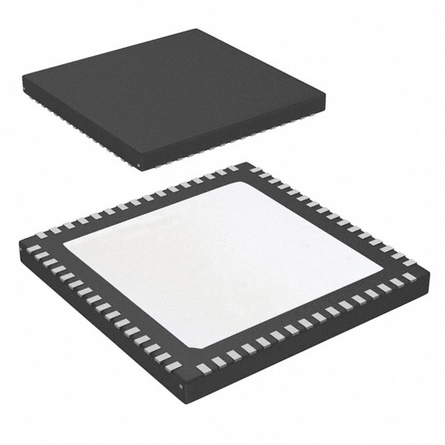
Silicon Labs EFM32G840F32G-E-QFN64

Part No.:
EFM32G840F32G-E-QFN64
Manufacturer:
Silicon Labs
Category:
Microcontrollers
Package:
64-VFQFN Exposed Pad
Datasheet:
AetrixEFM32G840F32G-E-QFN64.pdf
Description:
IC MCU 32BIT 32KB FLASH 64QFN
Quantity:
Payment:
Payment
Shipping:
Shipping

Inventory:4,764

Please send an inquiry. Send us your inquiry, and we will respond immediately.

Part Number
Quantity*
Price
Name*
Company
Email*
Comments

Product details

Overview

EFM32G840F32G-E-QFN64 from Silicon Labs is a 32-bit ARM Cortex-M3 microcontroller optimized for ultra-low-power battery-operated systems. It delivers 32 MHz operation, 32 kB Flash, 8 kB RAM, hardware AES encryption, and supports EM0–EM4 energy modes with 180 μA/MHz active current and 0.6 μA Stop mode current. It is used in smart metering, health wearables, and industrial sensor nodes requiring long battery life and autonomous peripheral operation.

For engineers reviewing the EFM32G840F32G-E-QFN64 datasheet, EFM32G840F32G-E-QFN64 pinout, EFM32G840F32G-E-QFN64 application, or EFM32G840F32G-E-QFN64 equivalent, key selection criteria include verified QFN64 package compatibility, confirmed 32 kB Flash/8 kB RAM configuration, validated low-energy UART and PRS autonomy in EM2, and documented 32.768 kHz RTC retention in Deep Sleep mode.

Technical Context

The EFM32G840F32G-E-QFN64 implements the ARM Cortex-M3 core with Memory Protection Unit and Wake-up Interrupt Controller, enabling deterministic real-time response and secure memory partitioning. Its Energy Management Unit (EMU) orchestrates five distinct energy modes (EM0–EM4), with peripherals like LEUART, RTC, and LETIMER retaining functionality down to EM2.

Peripheral Reflex System (PRS) enables CPU-free inter-peripheral signaling-e.g., ADC conversion completion triggering DMA transfer or TIMER compare event initiating DAC update-reducing wake cycles and system-level power consumption. Clock Management Unit (CMU) provides per-module clock gating and multi-oscillator support (HFXO, LFXO, HFRCO, LFRCO, ULFRCO) for precise timing control across operating modes.

Key Specifications

ParameterValue and Actual Design Meaning
CPU CoreARM Cortex-M3 @ 32 MHz - full 32-bit RISC execution with 1.25 DMIPS/MHz performance and MPU-based memory isolation.
Memory32 kB Flash / 8 kB RAM - sufficient for compact firmware with retained SRAM in Stop (EM3) and Deep Sleep (EM2) modes.
Power Consumption0.6 μA in Stop (EM3) with RAM/CPU retention - enables rapid wake-up (<2 µs) while preserving context for infrequent event handling.
Low-Energy PeripheralsLEUART + LETIMER + RTC active in EM2 - allows time-triggered communication and sensing without CPU involvement.
Analog Performance12-bit 1 Msps ADC (8 SE/4 diff channels) + 12-bit 500 ksps DAC (2 SE/1 diff) - supports precision sensor acquisition and analog output in battery-constrained designs.
SecurityHardware AES-128/256 accelerator (54/75 cycles) - offloads encryption from CPU, reducing latency and energy use in secure boot or data transmission.
PackageQFN64 (9 × 9 mm, 0.5 mm pitch) - surface-mount, thermally enhanced package suitable for space-constrained PCB layouts.

Pinout & Package

EFM32G840F32G-E-QFN64 is housed in a 64-pin QFN package (9 × 9 mm body, 0.5 mm pitch, exposed thermal pad). Pin functions are configurable via alternate function mapping, supporting flexible I/O routing across multiple peripheral interfaces.

Pin/TerminalCircuit RoleDesign Meaning
VDDCore Power Supply1.98–3.8 V main supply; powers CPU, RAM, and digital logic; requires local 100 nF decoupling.
VSSDigital GroundReference return path for digital I/O and core logic; must be connected to PCB ground plane.
PA0–PA7General Purpose I/OConfigurable GPIO with pull-up/down, drive strength, and interrupt capability; supports PRS input/output.
PC0–PC13Peripheral I/O MultiplexingShared with USART0/1/2, LEUART0, I²C0/1, ADC0, DAC0, ACMP0/1 - enables mixed-signal interface consolidation.
PF0–PF7Low-Energy Timer & RTC I/OSupports LETIMER output, RTC clock input (LFXO), and EM4 wake-up sources; retains function in Deep Sleep.
SWDIO/SWCLKDebug Interface2-pin Serial Wire Debug for programming and real-time trace; operates in EM0–EM2, disabled in EM3/EM4.

Key Features

FeatureDesign Value
Autonomous Peripheral Reflex System (PRS)Enables CPU-free signal chaining (e.g., ADC done → DMA fetch → TIMER update), cutting active time by up to 40% in sensor polling loops.
Multi-mode Energy Management (EM0–EM4)EM2 retains RTC, LETIMER, LEUART, and PRS while drawing ≤0.9 μA - ideal for periodic wake-up without full system restart.
Hardware AES AcceleratorExecutes AES-128 encryption in 54 cycles (vs. ~10k+ cycles in software), reducing active time and power per encrypted packet.
Configurable I/O Location MappingAllows remapping of USART, I²C, and timer pins to alternative GPIO ports - simplifies PCB layout and avoids routing congestion.
Integrated LCD ControllerDrives up to 4×40 segments with voltage boost and auto-contrast; operates autonomously in EM2 using internal charge pump.

Applications

Smart Utility MeteringWireless Health Sensor Node

Use Scenario: Battery-powered gas/water meter logging flow data hourly and transmitting via sub-GHz RF every 24 hours.

IC Role / Device Role / Timing Role: Main controller executing metering algorithms, managing RTC-triggered sampling, and driving LEUART for RF module handshaking.

Use Value: 0.6 μA Stop mode extends 10-year battery life; PRS-linked ADC→DMA→TIMER sequence eliminates CPU wake-ups during calibration pulses.

Use Scenario: Wearable ECG patch acquiring analog biopotentials, performing on-device filtering, and streaming processed data via BLE.

IC Role / Device Role / Timing Role: Signal acquisition hub with 12-bit ADC, real-time FIR filtering via Cortex-M3, and hardware AES for secure data upload.

Use Value: 1 Msps ADC captures high-fidelity waveforms; hardware AES reduces encryption latency by 98%, preserving BLE connection windows.

Industrial Predictive Maintenance SensorHome Automation Gateway Controller

Use Scenario: Vibration sensor node mounted on motor housing, capturing acceleration spectra and detecting bearing faults via FFT analysis.

IC Role / Device Role / Timing Role: Edge analytics processor running lightweight ML inference, with LETIMER-triggered sampling and RTC-scheduled uploads.

Use Value: EM2 operation with active LETIMER and ADC enables 10 ms burst sampling every 5 seconds at <1.2 μA average current.

Use Scenario: Zigbee-to-WiFi bridge aggregating data from 15+ smart switches/sensors and exposing REST API to cloud platform.

IC Role / Device Role / Timing Role: Protocol translation engine managing concurrent I²C (sensor hub), USART (Zigbee SoC), and SPI (WiFi module) interfaces.

Use Value: Configurable I/O mapping allows co-location of I²C and USART signals on same port group, reducing layer count and BOM cost.

Equivalent & Alternatives

The following parts are listed as comparable options for similar low-energy microcontroller applications.

Alternative PartTechnical DifferenceApplication DifferenceSelection Advice
EFM32G230F32G-E-QFN64Same QFN64 package, identical 32 kB Flash/8 kB RAM, but belongs to G230 series with fewer PRS channels (4 vs. 8) and no LCD controller.Lacks integrated LCD driver and reduced PRS flexibility - unsuitable for display-integrated or complex autonomous peripheral workflows.Select when display output is unnecessary and PRS routing complexity is low; verify peripheral count against design requirements.
EFM32GG11B120F1024GL120Higher-tier EFM32 Giant Gecko Gen11 device: ARM Cortex-M4, 1024 kB Flash, 128 kB RAM, QFN64, but higher active current (210 μA/MHz) and no EM4 Shutoff mode.Targets compute-intensive edge AI or audio processing; incompatible energy mode depth and not drop-in for EM4-dependent designs.Choose only if >32 kB Flash or FPU-assisted math is required; not a functional substitute for EM4 or ultra-low-quiescent use cases.

Compared with EFM32G230F32G-E-QFN64, the EFM32G840F32G-E-QFN64 offers full 8-channel PRS and LCD support for richer HMI; versus EFM32GG11B120F1024GL120, it trades raw performance for guaranteed sub-1 μA Deep Sleep and proven EM4 shutoff-critical for 10+ year sealed-battery deployments.

Availability

EFM32G840F32G-E-QFN64 is available at Aetrix Electronics and suitable for smart metering, wearable health monitoring, and industrial predictive maintenance applications requiring stable component supply, long-term lifecycle assurance, and qualified low-power MCU sourcing.

Supply support for EFM32G840F32G-E-QFN64 includes scheduled delivery planning, volume procurement assistance, BOM continuity management, traceable sourcing, and lifecycle availability coordination for OEM customers, industrial embedded developers, connected-device designers, and electronics production programs.

Manufacturer

Silicon Labs is a fabless semiconductor company specializing in low-power wireless and mixed-signal ICs for IoT, industrial, and consumer applications.

The EFM32 Gecko family was designed specifically for energy-constrained embedded systems, emphasizing autonomous peripheral operation, multi-mode energy management, and fast wake-up to maximize battery lifetime without sacrificing 32-bit performance.

FAQ

What is the maximum operating frequency and supported voltage range for the EFM32G840F32G-E-QFN64?

The EFM32G840F32G-E-QFN64 operates at up to 32 MHz across a supply voltage range of 1.98 V to 3.8 V. This range accommodates single-cell Li-ion, two-cell alkaline, or regulated 3.3 V systems. All specified current consumption values-including 180 μA/MHz in Run mode and 0.6 μA in Stop mode-are validated within this voltage window per the official EFM32G datasheet Rev. 2.20.

Does the EFM32G840F32G-E-QFN64 support hardware debugging, and what interface is used?

Yes, the EFM32G840F32G-E-QFN64 supports hardware debugging via a 2-pin Serial Wire Debug (SWD) interface (SWDIO and SWCLK pins), compliant with ARM CoreSight standards. It also includes a 1-pin Serial Wire Viewer (SWV) for real-time trace and profiling. Debug remains functional in EM0–EM2 energy modes but is disabled in EM3 and EM4 to preserve lowest possible leakage.

How many energy-saving modes does the EFM32G840F32G-E-QFN64 support, and which peripherals remain active in Deep Sleep (EM2)?

The EFM32G840F32G-E-QFN64 supports five energy modes: EM0 (Active), EM1 (Sleep), EM2 (Deep Sleep), EM3 (Stop), and EM4 (Shutoff). In EM2, the RTC, LETIMER, LEUART, PRS, and selected GPIOs remain fully operational while drawing ≤0.9 μA at 3 V-enabling time-triggered tasks without CPU intervention.

Is the EFM32G840F32G-E-QFN64 pin-compatible with other EFM32G QFN64 variants such as EFM32G230F32G-E-QFN64?

Yes, the EFM32G840F32G-E-QFN64 shares identical QFN64 mechanical dimensions, pin count, and pinout with EFM32G230F32G-E-QFN64 and EFM32G232F32G-E-QFP64 (TQFP variant). Electrical pin functions-including VDD, VSS, SWD, and primary GPIO groups-are functionally aligned per Silicon Labs' EFM32G pin definition documentation (Rev. 2.20, Section 5.3 and 5.7).

What analog peripherals are integrated into the EFM32G840F32G-E-QFN64, and what are their key specifications?

The EFM32G840F32G-E-QFN64 integrates a 12-bit 1 Msps ADC (8 single-ended or 4 differential inputs), a 12-bit 500 ksps DAC (2 single-ended or 1 differential output), two analog comparators (ACMP), and a supply voltage comparator (VCMP). These are all accessible in EM0–EM2 modes, with ADC offset error <±1.5 LSB and DAC INL <±0.5 LSB-validated per Electrical Characteristics section (Rev. 2.20, Table 4.10–4.13).

EFM32G840F32G-E-QFN64 Specifications

Product attributes
Attribute value
Manufacturer:
Silicon Labs
Package/Case:
64-VFQFN Exposed Pad
Series:
Gecko
Packaging:
Tray
Product Status:
Active
Programmable:
Not Verified
Core Processor:
ARM® Cortex®-M3
Core Size:
32-Bit Single-Core
Speed:
32MHz
Connectivity:
I2C, IrDA, SmartCard, SPI, UART/USART
Peripherals:
Brown-out Detect/Reset, DMA, LCD, POR, PWM, WDT
Number of I/O:
56
Program Memory Size:
32KB (32K x 8)
Program Memory Type:
FLASH
EEPROM Size:
-
RAM Size:
8K x 8
Voltage - Supply (Vcc/Vdd):
1.98V ~ 3.8V
Data Converters:
A/D 8x12b; D/A 2x12b
Oscillator Type:
Internal
Operating Temperature:
-40°C ~ 85°C (TA)
Grade:
-
Qualification:
-
Mounting Type:
Surface Mount
Supplier Device Package:

EFM32G840F32G-E-QFN64 FAQ

1.How can I place an order for EFM32G840F32G-E-QFN64 through Aetrix?

Please submit a Request for Quotation (RFQ) for EFM32G840F32G-E-QFN64 on Aetrix. Our sales agent will provide a competitive quotation and guide you through the order confirmation once you accept the terms.

2.Are the price and stock information for EFM32G840F32G-E-QFN64 reliable?

The price and inventory of EFM32G840F32G-E-QFN64 are updated periodically and may fluctuate due to market conditions. Stock and pricing data are typically refreshed every 24 hours. Quotation validity for EFM32G840F32G-E-QFN64 is usually 5 days.

3.What payment methods are accepted for EFM32G840F32G-E-QFN64?

We accept Wire Transfer, PayPal, Credit Card, Western Union, MoneyGram, and Escrow for EFM32G840F32G-E-QFN64 transactions.

Note: Certain payment methods may incur a processing fee.

4.How is shipping managed for EFM32G840F32G-E-QFN64?

EFM32G840F32G-E-QFN64 orders can be shipped via leading logistics carriers, including DHL, UPS, FedEx, TNT, or Registered Mail.

Once your EFM32G840F32G-E-QFN64 order is processed, you will receive an email with the shipment details and tracking number.

Note: Tracking information may take up to 24 hours to appear. Express delivery typically takes 3–5 business days.

5.How can I obtain technical support or documentation for EFM32G840F32G-E-QFN64?

For technical support, including EFM32G840F32G-E-QFN64 datasheets, pinout diagrams, or application guidance, please contact our engineering support team. They can provide detailed documentation and assistance for your EFM32G840F32G-E-QFN64 requirements.

6.How does Aetrix verify that EFM32G840F32G-E-QFN64 is sourced from the original manufacturer or authorized distributors?

All EFM32G840F32G-E-QFN64 products on Aetrix are procured from qualified distributors and authorized channels. Our dedicated quality assurance team conducts strict verification, including traceability checks and, if necessary, third-party testing. This ensures that EFM32G840F32G-E-QFN64 meets industry standards.

7.What is the process for return or replacement of EFM32G840F32G-E-QFN64?

All EFM32G840F32G-E-QFN64 units undergo pre-shipment inspection (PSI). If there is an issue with EFM32G840F32G-E-QFN64, returns or replacements are accepted under the following conditions:

1.Quantity discrepancies, incorrect items, or visible external defects (such as breakage or corrosion), acknowledged by Aetrix.

2.The issue is reported within 90 days of delivery.

3.The EFM32G840F32G-E-QFN64 part is unused and in its original packaging.

Return procedure for EFM32G840F32G-E-QFN64:

1.Submit a request within 90 days.

2.Obtain a Return Material Authorization (RMA) from Aetrix.

EFM32G840F32G-E-QFN64 Tags

  • EFM32G840F32G-E-QFN64
  • EFM32G840F32G-E-QFN64 PDF
  • EFM32G840F32G-E-QFN64 Datasheet
  • EFM32G840F32G-E-QFN64 Specifications
  • EFM32G840F32G-E-QFN64 Images
  • Silicon Labs
  • Silicon Labs EFM32G840F32G-E-QFN64
  • Buy EFM32G840F32G-E-QFN64
  • EFM32G840F32G-E-QFN64 Price
  • EFM32G840F32G-E-QFN64 Distributor
  • EFM32G840F32G-E-QFN64 Supplier
  • EFM32G840F32G-E-QFN64 Wholesale
Related Products
ATTINY4-TSHR
ATTINY4-TSHR

Microchip Technology

ATTINY10-TSHR
ATTINY10-TSHR

Microchip Technology

ATTINY10-TS8R
ATTINY10-TS8R

Microchip Technology

ATTINY202-SSNR
ATTINY202-SSNR

Microchip Technology

ATTINY202-SSFR
ATTINY202-SSFR

Microchip Technology

ATTINY402-SSNR
ATTINY402-SSNR

Microchip Technology

PIC16F15213T-I/MF
PIC16F15213T-I/MF

Microchip Technology

PIC16F15213-E/MF
PIC16F15213-E/MF

Microchip Technology

PIC10F200T-I/OT
PIC10F200T-I/OT

Microchip Technology

ATTINY412-SSNR
ATTINY412-SSNR

Microchip Technology

PIC10F202T-I/OT
PIC10F202T-I/OT

Microchip Technology

ATTINY404-SSNR
ATTINY404-SSNR

Microchip Technology

Tech Hub

Search

Search

PRODUCT

PRODUCT

PHONE

PHONE

USER

USER