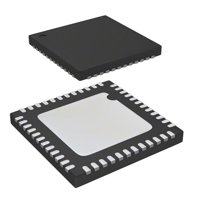
Silicon Labs EFM32PG1B200F256IM48-C0R
- Part No.:
- EFM32PG1B200F256IM48-C0R
- Manufacturer:
- Silicon Labs
- Category:
- Microcontrollers
- Package:
- 48-VFQFN Exposed Pad
- Datasheet:
-
EFM32PG1B200F256IM48-C0R.pdf
- Description:
- IC MCU 32BIT 256KB FLASH 48QFN
- Quantity:
- Payment:

- Shipping:

Inventory:1,600
Please send an inquiry. Send us your inquiry, and we will respond immediately.
Product details
Overview
EFM32PG1B200F256IM48-C0R from Silicon Labs is a 32-bit ARM Cortex-M4 microcontroller operating at up to 40 MHz with DSP extensions and FPU, featuring 256 kB flash, 32 kB RAM, integrated DC-DC converter, hardware AES/ECC/SHA crypto engine, and ultra-low energy modes including 0.58 μA EM4H hibernate with 128-byte RAM retention. It targets battery-powered IoT sensors and industrial edge nodes requiring secure, long-life operation.
For engineers reviewing the EFM32PG1B200F256IM48-C0R datasheet, EFM32PG1B200F256IM48-C0R pinout, EFM32PG1B200F256IM48-C0R application, or EFM32PG1B200F256IM48-C0R equivalent, key selection criteria include EM4H current draw, CRYOTIMER wake-up capability in hibernate, DC-DC efficiency at 200 mA load, 5 V-tolerant I/O compatibility, and PRS-enabled autonomous peripheral coordination without CPU wake-up.
Technical Context
The EFM32PG1B200F256IM48-C0R implements a flexible energy management architecture with five defined energy modes (EM0–EM4), where EM4H retains 128 bytes of RAM at 0.58 μA and supports CRYOTIMER wake-up via LFXO/LFRCO/ULFRCO. Its Peripheral Reflex System (PRS) enables hardware-triggered signal routing between 12-channel peripherals-including TIMER, RTCC, LETIMER, and ACMP-without CPU intervention.
It integrates dual oscillators (HFXO up to 40 MHz, LFXO 32.768 kHz) plus six internal RC sources (HFRCO, AUXHFRCO, LFRCO, ULFRCO), all managed by the Clock Management Unit (CMU) for dynamic clock gating. The crypto accelerator supports AES-128/256, NIST P-192/P-256/ECC-K163, and SHA-224/256 with DMA-triggered operation and GCM/CCM mode acceleration.
Key Specifications
| Parameter | Value and Actual Design Meaning |
|---|---|
| CPU Core | ARM Cortex-M4 @ 40 MHz with FPU and DSP extensions - enables real-time sensor fusion and floating-point control loops |
| Flash / RAM | 256 kB flash / 32 kB RAM - sufficient for secure bootloader, TLS stack, and firmware-over-the-air (FOTA) staging |
| Energy Mode 4H Current | 0.58 μA with 128-byte RAM retention - extends coin-cell battery life to >10 years in periodic wake-up sensing |
| DC-DC Output | 1.8 V output, 200 mA max - powers external sensors or RF transceivers directly from MCU regulator |
| Crypto Engine | AES-128/256, ECC-P256, SHA-256 - accelerates TLS handshake and firmware signature verification in <10 ms |
| I/O Voltage Tolerance | 5 V tolerant on all GPIO - simplifies interface to legacy 5 V sensors and logic without level shifters |
| Analog Peripherals | 12-bit 1 Msps ADC, 2× ACMP, IDAC (0.05–64 μA) - supports capacitive touch, battery voltage monitoring, and precision analog sensing |
Pinout & Package
EFM32PG1B200F256IM48-C0R uses a 7 mm × 7 mm QFN48 package with exposed thermal pad, rated for -40 °C to +125 °C junction temperature. Pin functions are configurable via port mapper and support multiple alternate functions per pin.
| Pin/Terminal | Circuit Role | Design Meaning |
|---|---|---|
| VDD, VSS | Power supply and ground | Single 1.85–3.8 V supply; VSS connects to thermal pad for thermal dissipation |
| IOVDD | I/O voltage reference | Independent 1.85–3.8 V rail enabling 5 V-tolerant operation regardless of core voltage |
| HFXO_P/N | High-frequency crystal input | Supports 38–40 MHz crystals for precise system timing and USB clock derivation |
| LFXO_P/N | Low-frequency crystal input | Drives RTCC and CRYOTIMER in EM2–EM4; enables calendar-based wake-up every second |
| PA0–PA7, PB0–PB7, PC0–PC7, PD0–PD7, PF0–PF7 | General-purpose I/O | 32 total GPIO with programmable drive strength, glitch filtering, and PRS routing capability |
| SWDIO / SWCLK | Debug interface | 2-pin Serial Wire Debug - allows full debug access with minimal PCB footprint |
| RESETn | Active-low reset input | Asynchronous reset with internal pull-up; compatible with open-drain reset supervisors |
Key Features
| Feature | Design Value |
|---|---|
| CRYOTIMER in EM4 | 32-bit wake-up timer operational in hibernate mode using ULFRCO (1 kHz), enabling sub-μA periodic sensing intervals |
| Peripheral Reflex System | 12-channel autonomous signal routing - allows ADC-triggered LED PWM or RTCC-alarm → GPIO toggle without CPU wake-up |
| Integrated DC-DC Converter | Buck regulator with bypass mode - maintains 90% efficiency down to 10 μA load and prevents brown-out during RF transmit bursts |
| Hardware Crypto Accelerator | Dedicated AES/GCM and ECC engines - offloads 100% of TLS record encryption from CPU, reducing active time by >65% |
| 5 V-Tolerant I/O | All GPIO pins withstand 5.5 V - eliminates external level shifters when interfacing with industrial 5 V sensors or actuators |
Applications
| Smart Sensor Node | Industrial Edge Controller |
|---|---|
Use Scenario: Wireless environmental monitor powered by CR2032 coin cell, sampling temperature/humidity every 5 minutes and transmitting via BLE. IC Role / Device Role: Main system controller managing sensor acquisition, crypto-secured data packaging, low-energy radio handshaking, and EM4H hibernation between samples. Use Value: 0.58 μA EM4H current and CRYOTIMER wake-up extend battery life beyond 12 years; integrated DC-DC powers external sensors at 1.8 V without external regulators. | Use Scenario: DIN-rail mounted PLC module collecting analog inputs from 4–20 mA field transmitters and controlling relay outputs over Modbus RTU. IC Role / Device Role: Real-time deterministic controller executing PID loops, isolating analog front-end, and managing dual UART interfaces (Modbus master/slave). Use Value: 40 MHz Cortex-M4 with FPU delivers 200 μs PID execution; 5 V-tolerant I/O interfaces directly to industrial transmitters; PRS links ADC conversion completion to UART TX start for zero-latency response. |
| Secure Wearable Health Device | Home Automation Hub |
Use Scenario: FDA-classified wearable measuring ECG and SpO₂, storing encrypted biometric logs locally before Bluetooth sync. IC Role / Device Role: Secure processing unit performing analog front-end control, cryptographic signing of health data, tamper-resistant storage, and low-power BLE advertising. Use Value: Hardware AES-256 and ECC-P256 enable FIPS-compliant key generation and signature in <5 ms; EM2 DeepSleep at 2.5 μA sustains continuous heart-rate monitoring with 7-day battery life. | Use Scenario: Zigbee-to-Matter bridge aggregating ZHA sensors and exposing them as Matter endpoints over Thread/Wi-Fi. IC Role / Device Role: Protocol translation gateway handling concurrent Zigbee 3.0 stack, Matter SDK, and secure OTA updates with rollback protection. Use Value: 256 kB flash accommodates dual-image OTA; CRYPTO engine accelerates Matter certificate chain validation; PRS synchronizes Zigbee MAC timer with Thread network beacon scheduling. |
Equivalent & Alternatives
The following parts are listed as comparable options for similar microcontroller applications.
| Alternative Part | Technical Difference | Application Difference | Selection Advice |
|---|---|---|---|
| EFM32PG1B200F256GM48-C0 | Same silicon, -40 °C to +85 °C temp grade, tape-and-reel packaging | Targeting commercial indoor applications without extended thermal requirements | Select when ambient operating temperature remains below 85 °C and RoHS-compliant tape-and-reel is preferred over cut-tape |
| EFM32PG1B200F256IM32-C01 | QFN32 package, 20 GPIO, no DC-DC converter, -40 °C to +125 °C | Suitable for space-constrained designs where DC-DC is omitted and thermal margin exceeds 125 °C junction | Choose for compact PCB layouts needing fewer I/O and no integrated regulator; verify external 1.8 V supply stability under 200 mA transient loads |
Compared with EFM32PG1B200F256GM48-C0, the EFM32PG1B200F256IM48-C0R offers extended temperature operation critical for automotive under-hood or industrial motor-control enclosures; versus EFM32PG1B200F256IM32-C01, it provides 12 additional GPIO and integrated DC-DC - eliminating external regulator BOM cost and layout area while enabling higher peripheral integration.
Availability
EFM32PG1B200F256IM48-C0R is available at Aetrix Electronics and suitable for industrial edge controllers, secure wearables, smart sensor nodes, and home automation hubs requiring stable component supply across extended temperature ranges and long production lifecycles.
Supply support for EFM32PG1B200F256IM48-C0R includes scheduled delivery planning, volume procurement assistance, BOM continuity management, traceable sourcing, and lifecycle availability coordination for OEM customers, industrial embedded developers, connected-device designers, and electronics production programs.
Manufacturer
Silicon Labs is a fabless semiconductor company specializing in secure, energy-efficient MCU, wireless SoC, and timing solutions for IoT and industrial markets.
The EFM32 Pearl Gecko product line was designed specifically for ultra-low-energy, secure embedded applications - combining ARM Cortex-M4 performance with hardware-accelerated cryptography and multi-mode energy management optimized for battery-operated edge devices.
FAQ
What is the maximum operating temperature specification for the EFM32PG1B200F256IM48-C0R?
The EFM32PG1B200F256IM48-C0R is qualified for operation from -40 °C to +125 °C junction temperature. This extended temperature grade makes it suitable for deployment in harsh environments such as industrial motor drives, automotive cabin modules, and outdoor infrastructure nodes where ambient heat dissipation is limited.
Does the EFM32PG1B200F256IM48-C0R include an integrated DC-DC converter?
Yes, the EFM32PG1B200F256IM48-C0R includes an integrated buck DC-DC converter capable of delivering up to 200 mA at 1.8 V. It operates efficiently across EM0–EM3 energy modes and enters bypass mode below 2.3 V input to maintain regulation - a feature confirmed in Section 4.1.4 of the official EFM32PG1 Data Sheet Rev. 1.3.
How much RAM is retained in EM4H mode on the EFM32PG1B200F256IM48-C0R?
The EFM32PG1B200F256IM48-C0R retains 128 bytes of RAM in EM4H hibernate mode while drawing only 0.58 μA. This dedicated retention memory is accessible upon wake-up and is used to store critical state variables, timestamps, or cryptographic context - enabling rapid resumption without full reinitialization.
Can the EFM32PG1B200F256IM48-C0R operate with a 5 V I/O interface?
Yes, all GPIO pins on the EFM32PG1B200F256IM48-C0R are 5 V tolerant when IOVDD is supplied within its 1.85–3.8 V range. This allows direct connection to 5 V sensors, logic ICs, or industrial field buses without external level-shifting circuitry - a feature explicitly documented in Section 4.1.10 of the EFM32PG1 Data Sheet.
What cryptographic algorithms are accelerated by the hardware CRYPTO engine in the EFM32PG1B200F256IM48-C0R?
The hardware CRYPTO engine in the EFM32PG1B200F256IM48-C0R accelerates AES-128/256 (ECB, CTR, CBC, GCM, CCM), ECC over NIST P-192/P-224/P-256 and K-163/K-233 curves, and SHA-1/SHA-224/SHA-256. These capabilities are verified in Section 3.7.2 and Table 4.1.7 of the EFM32PG1 Data Sheet Rev. 1.3.
EFM32PG1B200F256IM48-C0R Specifications
- Product attributes
- Attribute value
- Manufacturer:
- Silicon Labs
- Package/Case:
- 48-VFQFN Exposed Pad
- Series:
- Pearl Gecko
- Packaging:
- Tape & Reel (TR)
- Product Status:
- Active
- Programmable:
- Not Verified
- Core Processor:
- ARM® Cortex®-M4
- Core Size:
- 32-Bit Single-Core
- Speed:
- 40MHz
- Connectivity:
- I2C, IrDA, LINbus, SmartCard, SPI, UART/USART
- Peripherals:
- Brown-out Detect/Reset, DMA, I2S, POR, PWM, WDT
- Number of I/O:
- 32
- Program Memory Size:
- 256KB (256K x 8)
- Program Memory Type:
- FLASH
- EEPROM Size:
- -
- RAM Size:
- 32K x 8
- Voltage - Supply (Vcc/Vdd):
- 1.85V ~ 3.8V
- Data Converters:
- A/D 24x12b
- Oscillator Type:
- Internal
- Operating Temperature:
- -40°C ~ 125°C (TJ)
- Grade:
- -
- Qualification:
- -
- Mounting Type:
- Surface Mount
- Supplier Device Package:
EFM32PG1B200F256IM48-C0R FAQ
1.How can I place an order for EFM32PG1B200F256IM48-C0R through Aetrix?
Please submit a Request for Quotation (RFQ) for EFM32PG1B200F256IM48-C0R on Aetrix. Our sales agent will provide a competitive quotation and guide you through the order confirmation once you accept the terms.
2.Are the price and stock information for EFM32PG1B200F256IM48-C0R reliable?
The price and inventory of EFM32PG1B200F256IM48-C0R are updated periodically and may fluctuate due to market conditions. Stock and pricing data are typically refreshed every 24 hours. Quotation validity for EFM32PG1B200F256IM48-C0R is usually 5 days.
3.What payment methods are accepted for EFM32PG1B200F256IM48-C0R?
We accept Wire Transfer, PayPal, Credit Card, Western Union, MoneyGram, and Escrow for EFM32PG1B200F256IM48-C0R transactions.
Note: Certain payment methods may incur a processing fee.
4.How is shipping managed for EFM32PG1B200F256IM48-C0R?
EFM32PG1B200F256IM48-C0R orders can be shipped via leading logistics carriers, including DHL, UPS, FedEx, TNT, or Registered Mail.
Once your EFM32PG1B200F256IM48-C0R order is processed, you will receive an email with the shipment details and tracking number.
Note: Tracking information may take up to 24 hours to appear. Express delivery typically takes 3–5 business days.
5.How can I obtain technical support or documentation for EFM32PG1B200F256IM48-C0R?
For technical support, including EFM32PG1B200F256IM48-C0R datasheets, pinout diagrams, or application guidance, please contact our engineering support team. They can provide detailed documentation and assistance for your EFM32PG1B200F256IM48-C0R requirements.
6.How does Aetrix verify that EFM32PG1B200F256IM48-C0R is sourced from the original manufacturer or authorized distributors?
All EFM32PG1B200F256IM48-C0R products on Aetrix are procured from qualified distributors and authorized channels. Our dedicated quality assurance team conducts strict verification, including traceability checks and, if necessary, third-party testing. This ensures that EFM32PG1B200F256IM48-C0R meets industry standards.
7.What is the process for return or replacement of EFM32PG1B200F256IM48-C0R?
All EFM32PG1B200F256IM48-C0R units undergo pre-shipment inspection (PSI). If there is an issue with EFM32PG1B200F256IM48-C0R, returns or replacements are accepted under the following conditions:
1.Quantity discrepancies, incorrect items, or visible external defects (such as breakage or corrosion), acknowledged by Aetrix.
2.The issue is reported within 90 days of delivery.
3.The EFM32PG1B200F256IM48-C0R part is unused and in its original packaging.
Return procedure for EFM32PG1B200F256IM48-C0R:
1.Submit a request within 90 days.
2.Obtain a Return Material Authorization (RMA) from Aetrix.
EFM32PG1B200F256IM48-C0R Tags

-
ATTINY4-TSHR
Microchip Technology

-
ATTINY10-TSHR
Microchip Technology

-
ATTINY10-TS8R
Microchip Technology

-
ATTINY202-SSNR
Microchip Technology

-
ATTINY202-SSFR
Microchip Technology

-
ATTINY402-SSNR
Microchip Technology

-
PIC16F15213T-I/MF
Microchip Technology

-
PIC16F15213-E/MF
Microchip Technology

-
PIC10F200T-I/OT
Microchip Technology

-
ATTINY412-SSNR
Microchip Technology

-
PIC10F202T-I/OT
Microchip Technology

-
ATTINY404-SSNR
Microchip Technology
Tech Hub

Comparator circuit design covering voltage thresholds, input limits, open-collector outputs, LM393 wiring, op-amp differences, hysteresis, timing, window detection and practical fault diagnosis.
Schmitt triggers use separate rising and falling thresholds to stabilize slow or noisy signals. This guide covers hysteresis, 74HC14 and 74HCT14 selection, comparator calculations, RC oscillators and p…
Counterfeit components can hide behind convincing markings and passing basic function tests. This engineering reference covers source traceability, external inspection, X-ray, XRF, electrical testing, …
A practical engineering and sourcing framework covering lifecycle verification, lifetime-buy calculations, replacement qualification, supplier checks and counterfeit-risk controls.
TTL and CMOS logic families differ in thresholds, loading, output drive, power and timing. This engineering guide compares 74HC and 74HCT, calculates noise margins and checks 3.3 V/5 V compatibility.
A practical engineering guide to 3.3V and 5V logic compatibility, input thresholds, resistor dividers, translator ICs, MOSFET level shifting, I2C pull-ups, timing limits and power-sequencing risks.
The 74HC595 uses push-pull logic outputs, while the TPIC6B595 uses 50 V open-drain DMOS sinks for higher-power loads. This guide compares timing, current limits, 3.3 V interfacing, load wiring, thermal…
The 74HC595 converts serial data into eight stable parallel outputs. This guide covers pin functions, shift and storage timing, OE and MR behavior, drive-current limits, cascading, voltage compatibilit…
A technical comparison of level-sensitive latches and edge-triggered flip-flops, covering timing windows, setup and hold limits, master–slave operation, time borrowing, race-through, HDL inference and…
A D latch stores one bit while Enable controls when data can pass. This reference covers gate-level operation, truth tables, transparency, setup and hold timing, LE versus OE, common ICs and practical …