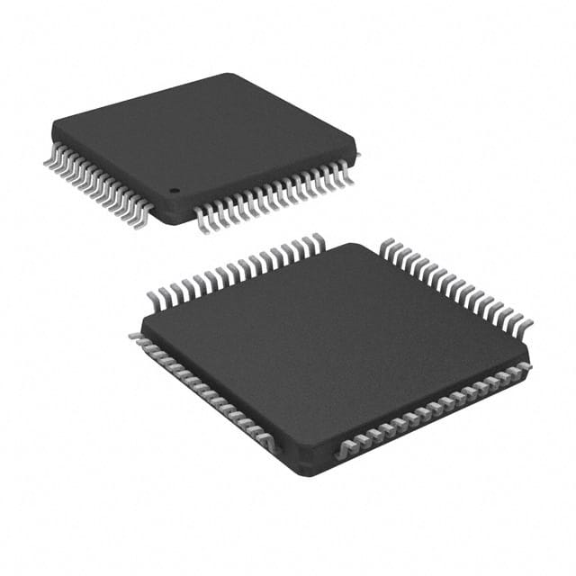
Silicon Labs EFM32TG11B320F128IQ64-B
- Part No.:
- EFM32TG11B320F128IQ64-B
- Manufacturer:
- Silicon Labs
- Category:
- Microcontrollers
- Package:
- 64-TQFP
- Datasheet:
-
EFM32TG11B320F128IQ64-B.pdf
- Description:
- IC MCU 32BIT 128KB FLASH 64TQFP
- Quantity:
- Payment:

- Shipping:

Inventory:4,674
Please send an inquiry. Send us your inquiry, and we will respond immediately.
Product details
Overview
EFM32TG11B320F128IQ64-B from Silicon Labs is a 32-bit ARM Cortex-M0+ microcontroller operating at up to 48 MHz, featuring 128 kB flash, 32 kB RAM, CAN 2.0B controller (up to 1 Mbps), hardware cryptographic engine (AES-128/256, ECC, SHA-256, TRNG), and ultra-low-power operation (1.30 µA in EM2 Deep Sleep with RTCC running). It targets battery-powered smart energy meters and industrial edge sensors requiring secure, low-energy connectivity.
For engineers reviewing the EFM32TG11B320F128IQ64-B datasheet, EFM32TG11B320F128IQ64-B pinout, EFM32TG11B320F128IQ64-B application, or EFM32TG11B320F128IQ64-B equivalent, key selection criteria include extended temperature support (–40 °C to +125 °C), TQFP64 package with 53 GPIOs, absence of integrated DC-DC converter, and LCD driver capability - all confirmed for this exact ordering part number.
Technical Context
The EFM32TG11B320F128IQ64-B implements a dual-domain power architecture: primary domain powers core and high-speed peripherals in EM0–EM3, while backup domain maintains RTCC and retention registers across all energy modes including EM4S. Its CAN controller supports full CAN 2.0A/B frame formats and bit rates up to 1 Mbps with programmable timing and loopback testing.
Security is enforced via dedicated CRYPTO accelerator with deterministic AES encryption cycles, SMU-based peripheral access control, and TRNG entropy source feeding both cryptographic operations and secure boot. Analog subsystem includes 12-bit 1 Msps ADC, dual 12-bit VDACs, four OPAMPs, and CSEN supporting up to 38 capacitive touch inputs with wake-on-touch in EM2.
Key Specifications
| Parameter | Value and Actual Design Meaning |
|---|---|
| CPU Core | ARM Cortex-M0+ @ 48 MHz - delivers deterministic real-time response with <2.1 µs interrupt latency and MPU-enforced memory protection. |
| Memory | 128 kB flash / 32 kB RAM - supports field firmware updates via UART bootloader and retains full RAM content in EM2 Deep Sleep mode. |
| Energy Modes | EM0 (37 µA/MHz), EM2 (1.30 µA with RTCC active), EM4S (20 nA) - enables multi-year battery life in metering and sensor applications. |
| CAN Interface | CAN 2.0B controller, 1 Mbps max bit rate - provides robust automotive-grade serial bus communication with hardware message filtering and FIFO buffering. |
| Cryptographic Engine | AES-128/256, ECC (P192/P256), SHA-224/256, TRNG - accelerates TLS handshake, secure boot verification, and firmware signature validation in under 100 µs. |
| Operating Range | 1.8 V to 3.8 V supply, –40 °C to +125 °C junction temperature - qualified for harsh industrial environments without derating. |
| Package & I/O | TQFP64 (10 × 10 mm), 53 GPIOs with 5 V tolerance on select pins - enables direct interfacing with legacy 5 V logic and simplifies level-shifter elimination. |
Pinout & Package
TQFP64 package (10 × 10 mm, 0.5 mm pitch), RoHS-compliant, with exposed thermal pad. Pin 1 marked by dot; pin numbering follows standard counter-clockwise sequence starting from top-left corner.
| Pin/Terminal | Circuit Role | Design Meaning |
|---|---|---|
| VDD | Digital supply input | 1.8–3.8 V main power rail; decoupled per datasheet layout guidelines to ensure stable EM0–EM4 operation. |
| AVDD | Analog supply input | Independent analog rail; must be ≥1.8 V and filtered separately to maintain 12-bit ADC/VADC accuracy. |
| IOVDD0 | I/O voltage reference | Configurable 1.8–3.8 V output; sets logic thresholds and enables 5 V-tolerant operation on designated GPIOs. |
| RESETn | Active-low reset input | Asynchronous reset assertion halts CPU, clears registers, and forces boot from reset vector; debounced internally. |
| CAN_TX / CAN_RX | CAN differential signal pair | Dedicated pins for CAN physical layer interface; require external 120 Ω termination and common-mode choke for EMC compliance. |
| PA0–PA15, PB0–PB15, etc. | Configurable GPIO bank | 53 total GPIOs support peripheral routing (USART, I2C, LEUART, timers); each pin configurable as push-pull, open-drain, or analog. |
Key Features
| Feature | Design Value |
|---|---|
| Hardware Cryptography Accelerator | Offloads AES-128/256 encryption/decryption in <100 cycles per block, enabling sub-millisecond TLS record processing without CPU overhead. |
| Low-Energy Sensor Interface (LESENSE) | Autonomously monitors up to 16 sensors (capacitive, resistive, inductive) in EM2 Deep Sleep, triggering wake-up only on threshold violation. |
| Capacitive Sensing (CSEN) | Current-based sensing with 38-input support and built-in wake-on-touch; achieves <5 µA active current during continuous button scanning. |
| Integrated LCD Controller | Drives up to 8 × 32 segments with internal voltage boost and contrast control; operates fully in EM2 with no CPU intervention. |
| Peripheral Reflex System (PRS) | Enables autonomous peripheral-to-peripheral signaling (e.g., ADC trigger → DMA transfer → CRYPTO start) without CPU involvement or IRQ latency. |
Applications
| Smart Energy Metering | Industrial Edge Sensor Node |
|---|---|
|
Use Scenario: Utility-grade electricity meter with tamper detection, time-of-use billing, and HAN communication via CAN or LEUART. IC Role / Device Role / Timing Role: Main system controller executing metrology algorithms, managing secure firmware updates, and maintaining RTC/calendar across power loss via backup domain. Use Value: 1.30 µA EM2 current extends battery backup to >10 years; hardware TRNG and SMU enforce regulatory compliance (IEC 62056, DLMS/COSEM). |
Use Scenario: Wireless vibration/temperature node in predictive maintenance system, reporting via CAN to gateway with local anomaly detection. IC Role / Device Role / Timing Role: Real-time data acquisition hub with synchronized ADC sampling, FFT preprocessing, and encrypted CAN frame generation. Use Value: CSEN + LESENSE enable self-calibrating sensor interface; PRS-driven ADC→CRYPTO flow reduces active time by 68% versus polled implementation. |
| Home Automation Gateway | Medical Wearable Monitor |
|
Use Scenario: Zigbee/Z-Wave bridge aggregating sensor data and translating to CAN-based HVAC or lighting control bus. IC Role / Device Role / Timing Role: Protocol translation engine with dual-bus isolation (Zigbee UART ↔ CAN), secure OTA update handler, and LCD status display. Use Value: Integrated LCD driver eliminates external display controller; CAN 2.0B ensures interoperability with legacy building automation systems. |
Use Scenario: ECG/PPG patch with dry-electrode sensing, motion artifact compensation, and Bluetooth LE telemetry. IC Role / Device Role / Timing Role: Low-noise analog front-end controller with OPAMP-configured instrumentation amplifier, 12-bit ADC oversampling, and secure health data packaging. Use Value: 4 × OPAMPs support simultaneous biopotential and impedance measurement; TRNG satisfies FDA cybersecurity guidance for Class II devices. |
Equivalent & Alternatives
The following parts are listed as comparable options for similar microcontroller applications.
| Alternative Part | Technical Difference | Application Difference | Selection Advice |
|---|---|---|---|
| EFM32TG11B520F128IQ64-B | Includes integrated DC-DC buck converter; otherwise identical flash/RAM/CAN/crypto/performance specs. | Better suited for systems with wide input voltage range (e.g., 3.3–5 V battery or adapter input) where DC-DC efficiency gain justifies added BOM cost. | Select EFM32TG11B520F128IQ64-B when >10% system-level power reduction is required and external inductor/capacitor placement is feasible. |
| EFM32PG12B500F1024GL125-B | ARM Cortex-M4F core, 1024 kB flash, 256 kB RAM, no CAN, adds FPU and higher-speed USB/USART; operates at same temp grade. | Targets computationally intensive edge AI inference or motor control where CAN is not needed but floating-point math and larger code footprint are critical. | Choose EFM32PG12B500F1024GL125-B only if application requires >10× more flash or hardware FPU - not a drop-in replacement for CAN-dependent designs. |
Compared with EFM32TG11B520F128IQ64-B, the EFM32TG11B320F128IQ64-B trades DC-DC integration for lower system BOM cost and simpler layout, while retaining identical security, timing, and analog capabilities. Versus EFM32PG12B500F1024GL125-B, it offers CAN-native control at lower power and cost but lacks FPU and large memory - making it optimal for secure, battery-operated CAN endpoints.
Availability
EFM32TG11B320F128IQ64-B is available at Aetrix Electronics and suitable for smart energy metering, industrial sensor nodes, home automation gateways, and medical wearable monitors requiring stable component supply across extended temperature ranges and long product lifecycles.
Supply support for EFM32TG11B320F128IQ64-B includes scheduled delivery planning, volume procurement assistance, BOM continuity management, traceable sourcing, and lifecycle availability coordination for OEM customers, industrial embedded developers, connected-device designers, and electronics production programs.
Manufacturer
Silicon Labs is a fabless semiconductor company specializing in low-power wireless SoCs, timing solutions, and secure MCU platforms for IoT and industrial applications.
The EFM32 Tiny Gecko Series 1 product line was designed specifically for ultra-low-energy, secure, battery-operated edge devices - integrating CAN, crypto acceleration, and autonomous analog peripherals into a single die optimized for EM2/EM4 dominance.
FAQ
What is the maximum CAN bit rate supported by the EFM32TG11B320F128IQ64-B?
The EFM32TG11B320F128IQ64-B supports CAN 2.0B protocol with a maximum bit rate of 1 Mbps. This is achieved using the dedicated CAN controller with programmable timing registers and hardware message filtering, validated across the full –40 °C to +125 °C operating range. The CAN peripheral operates independently in EM2 Deep Sleep mode when configured with appropriate clock sources.
Does the EFM32TG11B320F128IQ64-B include an integrated DC-DC converter?
No, the EFM32TG11B320F128IQ64-B does not include an integrated DC-DC buck converter. This is explicitly indicated by the "3" in the feature set code (B320), distinguishing it from "B520" variants that do include DC-DC. Power must be supplied externally within the 1.8–3.8 V range, with proper decoupling per the datasheet recommendations.
How many GPIO pins are available on the EFM32TG11B320F128IQ64-B in the TQFP64 package?
The EFM32TG11B320F128IQ64-B provides 53 general-purpose I/O pins in its TQFP64 package. These pins support multiple configurations including push-pull, open-drain, pull-up/down, input filtering, and 5 V tolerance on designated signals - all configurable per-pin via the GPIO register set and routable to peripherals via the Digital Port Mapper.
What cryptographic algorithms are accelerated by the hardware CRYPTO engine in the EFM32TG11B320F128IQ64-B?
The hardware CRYPTO engine in the EFM32TG11B320F128IQ64-B accelerates AES-128 and AES-256 encryption/decryption, ECC over NIST P-192 and P-256 curves, SHA-1 and SHA-2 (SHA-224 and SHA-256), and provides a True Random Number Generator (TRNG) compliant with NIST SP 800-90B. All operations execute in constant time with dedicated register interfaces.
Is the EFM32TG11B320F128IQ64-B qualified for extended temperature operation?
Yes, the EFM32TG11B320F128IQ64-B is qualified for extended temperature operation from –40 °C to +125 °C (junction temperature), as indicated by the "I" in the ordering code suffix. This qualification covers all specified electrical characteristics including flash programming, RTC accuracy, CAN timing, and cryptographic operation - with no derating required across the full range.
EFM32TG11B320F128IQ64-B Specifications
- Product attributes
- Attribute value
- Manufacturer:
- Silicon Labs
- Package/Case:
- 64-TQFP
- Series:
- Tiny Gecko 1
- Packaging:
- Tray
- Product Status:
- Active
- Programmable:
- Not Verified
- Core Processor:
- ARM® Cortex®-M0+
- Core Size:
- 32-Bit Single-Core
- Speed:
- 48MHz
- Connectivity:
- CANbus, I2C, IrDA, LINbus, SmartCard, SPI, UART/USART
- Peripherals:
- Brown-out Detect/Reset, DMA, I2S, LCD, POR, PWM, WDT
- Number of I/O:
- 53
- Program Memory Size:
- 128KB (128K x 8)
- Program Memory Type:
- FLASH
- EEPROM Size:
- -
- RAM Size:
- 32K x 8
- Voltage - Supply (Vcc/Vdd):
- 1.8V ~ 3.8V
- Data Converters:
- A/D 12bit SAR; D/A 12bit
- Oscillator Type:
- Internal
- Operating Temperature:
- -40°C ~ 125°C (TJ)
- Grade:
- -
- Qualification:
- -
- Mounting Type:
- Surface Mount
- Supplier Device Package:
EFM32TG11B320F128IQ64-B FAQ
1.How can I place an order for EFM32TG11B320F128IQ64-B through Aetrix?
Please submit a Request for Quotation (RFQ) for EFM32TG11B320F128IQ64-B on Aetrix. Our sales agent will provide a competitive quotation and guide you through the order confirmation once you accept the terms.
2.Are the price and stock information for EFM32TG11B320F128IQ64-B reliable?
The price and inventory of EFM32TG11B320F128IQ64-B are updated periodically and may fluctuate due to market conditions. Stock and pricing data are typically refreshed every 24 hours. Quotation validity for EFM32TG11B320F128IQ64-B is usually 5 days.
3.What payment methods are accepted for EFM32TG11B320F128IQ64-B?
We accept Wire Transfer, PayPal, Credit Card, Western Union, MoneyGram, and Escrow for EFM32TG11B320F128IQ64-B transactions.
Note: Certain payment methods may incur a processing fee.
4.How is shipping managed for EFM32TG11B320F128IQ64-B?
EFM32TG11B320F128IQ64-B orders can be shipped via leading logistics carriers, including DHL, UPS, FedEx, TNT, or Registered Mail.
Once your EFM32TG11B320F128IQ64-B order is processed, you will receive an email with the shipment details and tracking number.
Note: Tracking information may take up to 24 hours to appear. Express delivery typically takes 3–5 business days.
5.How can I obtain technical support or documentation for EFM32TG11B320F128IQ64-B?
For technical support, including EFM32TG11B320F128IQ64-B datasheets, pinout diagrams, or application guidance, please contact our engineering support team. They can provide detailed documentation and assistance for your EFM32TG11B320F128IQ64-B requirements.
6.How does Aetrix verify that EFM32TG11B320F128IQ64-B is sourced from the original manufacturer or authorized distributors?
All EFM32TG11B320F128IQ64-B products on Aetrix are procured from qualified distributors and authorized channels. Our dedicated quality assurance team conducts strict verification, including traceability checks and, if necessary, third-party testing. This ensures that EFM32TG11B320F128IQ64-B meets industry standards.
7.What is the process for return or replacement of EFM32TG11B320F128IQ64-B?
All EFM32TG11B320F128IQ64-B units undergo pre-shipment inspection (PSI). If there is an issue with EFM32TG11B320F128IQ64-B, returns or replacements are accepted under the following conditions:
1.Quantity discrepancies, incorrect items, or visible external defects (such as breakage or corrosion), acknowledged by Aetrix.
2.The issue is reported within 90 days of delivery.
3.The EFM32TG11B320F128IQ64-B part is unused and in its original packaging.
Return procedure for EFM32TG11B320F128IQ64-B:
1.Submit a request within 90 days.
2.Obtain a Return Material Authorization (RMA) from Aetrix.
EFM32TG11B320F128IQ64-B Tags

-
ATTINY4-TSHR
Microchip Technology

-
ATTINY10-TSHR
Microchip Technology

-
ATTINY10-TS8R
Microchip Technology

-
ATTINY202-SSNR
Microchip Technology

-
ATTINY202-SSFR
Microchip Technology

-
ATTINY402-SSNR
Microchip Technology

-
PIC16F15213T-I/MF
Microchip Technology

-
PIC16F15213-E/MF
Microchip Technology

-
PIC10F200T-I/OT
Microchip Technology

-
ATTINY412-SSNR
Microchip Technology

-
PIC10F202T-I/OT
Microchip Technology

-
ATTINY404-SSNR
Microchip Technology
Tech Hub

Comparator circuit design covering voltage thresholds, input limits, open-collector outputs, LM393 wiring, op-amp differences, hysteresis, timing, window detection and practical fault diagnosis.
Schmitt triggers use separate rising and falling thresholds to stabilize slow or noisy signals. This guide covers hysteresis, 74HC14 and 74HCT14 selection, comparator calculations, RC oscillators and p…
Counterfeit components can hide behind convincing markings and passing basic function tests. This engineering reference covers source traceability, external inspection, X-ray, XRF, electrical testing, …
A practical engineering and sourcing framework covering lifecycle verification, lifetime-buy calculations, replacement qualification, supplier checks and counterfeit-risk controls.
TTL and CMOS logic families differ in thresholds, loading, output drive, power and timing. This engineering guide compares 74HC and 74HCT, calculates noise margins and checks 3.3 V/5 V compatibility.
A practical engineering guide to 3.3V and 5V logic compatibility, input thresholds, resistor dividers, translator ICs, MOSFET level shifting, I2C pull-ups, timing limits and power-sequencing risks.
The 74HC595 uses push-pull logic outputs, while the TPIC6B595 uses 50 V open-drain DMOS sinks for higher-power loads. This guide compares timing, current limits, 3.3 V interfacing, load wiring, thermal…
The 74HC595 converts serial data into eight stable parallel outputs. This guide covers pin functions, shift and storage timing, OE and MR behavior, drive-current limits, cascading, voltage compatibilit…
A technical comparison of level-sensitive latches and edge-triggered flip-flops, covering timing windows, setup and hold limits, master–slave operation, time borrowing, race-through, HDL inference and…
A D latch stores one bit while Enable controls when data can pass. This reference covers gate-level operation, truth tables, transparency, setup and hold timing, LE versus OE, common ICs and practical …