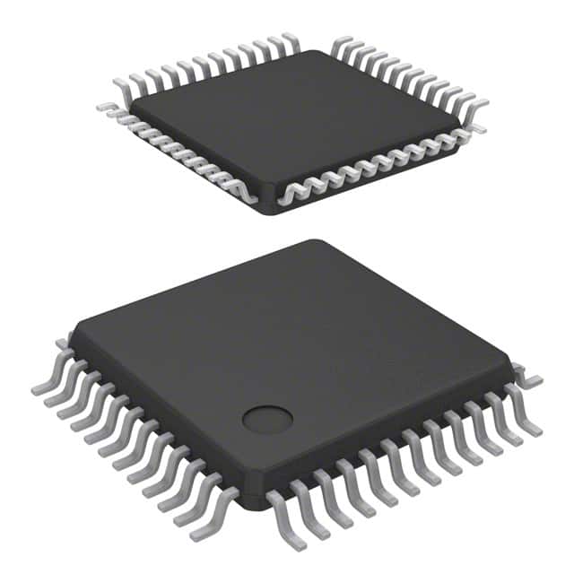
Silicon Labs EFM8UB20F32G-B-QFP48R
- Part No.:
- EFM8UB20F32G-B-QFP48R
- Manufacturer:
- Silicon Labs
- Category:
- Microcontrollers
- Package:
- 48-TQFP
- Datasheet:
-
EFM8UB20F32G-B-QFP48R.pdf
- Description:
- IC MCU 8BIT 32KB FLASH 48TQFP
- Quantity:
- Payment:

- Shipping:

Inventory:2,678
Please send an inquiry. Send us your inquiry, and we will respond immediately.
Product details
Overview
EFM8UB20F32G-B-QFP48R from Silicon Labs is a crystal-less USB 2.0 full/low-speed 8-bit MCU with pipelined CIP-51 core (48 MHz), 32 KB flash, 2304 bytes RAM, 40 multifunction I/O pins, and integrated 10-bit differential ADC with temperature sensor - designed for embedded USB peripherals, dongles, and communication bridges operating at 2.65–3.6 V.
For engineers reviewing the EFM8UB20F32G-B-QFP48R datasheet, EFM8UB20F32G-B-QFP48R pinout, EFM8UB20F32G-B-QFP48R application, or EFM8UB20F32G-B-QFP48R equivalent, key selection criteria include USB clock recovery accuracy (±0.25%), on-chip 5 V-to-3.3 V LDO, dual UARTs with 3-byte FIFO, and QFP48 package compatibility with legacy 8051 toolchains and debug via C2 interface.
Technical Context
The EFM8UB20F32G-B-QFP48R implements a fully compatible 8051 instruction set with 70% of instructions executing in 1–2 clock cycles, paired with a priority crossbar for flexible peripheral routing to its 40 I/O pins. Its USB 2.0 function controller integrates a transceiver, 1 KB FIFO, and clock recovery - enabling crystal-free operation without external components.
It features two internal oscillators (48 MHz HFOSC0 with ±0.25% USB-recovered accuracy and 80 kHz LFOSC0), six 16-bit timers, five-channel PCA supporting PWM/capture/frequency output, and a 10-bit SAR ADC with 500 ksps throughput, programmable window comparator, and integrated temperature sensor - all operational during debugging.
Key Specifications
| Parameter | Value and Actual Design Meaning |
|---|---|
| Core | Pipelined CIP-51 8051 running up to 48 MHz; enables real-time USB packet handling and deterministic interrupt latency. |
| Flash / RAM | 32 KB in-system reprogrammable flash and 2304 bytes RAM (256 standard + 2048 XRAM); supports field firmware updates and data logging. |
| USB Interface | Full/low-speed USB 2.0 function controller with 1 KB FIFO, integrated transceiver, and clock recovery; eliminates external crystal and matching components. |
| ADC | 10-bit differential SAR ADC with 500 ksps throughput, 32-channel analog mux, and integrated temperature sensor; enables precision sensor monitoring without external ICs. |
| Oscillators | Internal 48 MHz oscillator (±0.25% with USB clock recovery) and 80 kHz low-frequency oscillator; provides accurate timing for USB, UART, and low-power suspend modes. |
| I/O & Peripherals | 40 multifunction I/O pins with flexible crossbar routing; supports dual UARTs (3-byte RX FIFO), SPI, two SMBus/I²C, 5-channel PCA, and two analog comparators. |
| Power Management | On-chip 5 V-to-3.3 V LDO regulator, brown-out detector, power-on reset, and five low-power modes (Idle/Suspend/Stop/Shutdown); simplifies power design for USB bus-powered devices. |
Pinout & Package
EFM8UB20F32G-B-QFP48R is housed in a 48-pin Quad Flat Package (QFP48) with 0.5 mm pitch, RoHS-compliant, lead-free finish, and -40°C to +85°C industrial temperature rating.
| Pin/Terminal | Circuit Role | Design Meaning |
|---|---|---|
| VDD, VREGIN, GND | Power supply inputs | VDD (2.65–3.6 V) powers digital/analog circuits; VREGIN (2.7–5.25 V) feeds internal 5V-to-3.3V LDO; GND provides reference return. |
| D+, D-, VBUS | USB physical layer | D+/D- connect directly to USB connector; VBUS detects host presence and enables USB functionality automatically. |
| C2CK, C2D | C2 debug interface | 2-wire non-intrusive in-circuit debugging using production MCU; C2D shares P3.0 in QFP48 package. |
| P0.0–P3.7, P4.0–P4.7 | General-purpose I/O | Up to 40 pins configurable as GPIO, analog input, or routed to UART/SPI/I²C/USB/CMP via priority crossbar. |
| XTAL1, XTAL2 | External crystal interface | Supports optional 0.02–30 MHz crystal for precise timing when USB clock recovery is insufficient. |
| RSTb | Active-low reset input | Drives device into reset state; weak pullup enabled; compatible with standard reset button or supervisor ICs. |
Key Features
| Feature | Design Value |
|---|---|
| Crystal-less USB operation | Integrated 48 MHz oscillator with USB clock recovery achieves ±0.25% accuracy - eliminates external crystal, load capacitors, and layout constraints. |
| Pre-loaded USB bootloader | Resides in last three flash pages; enables firmware updates over USB without external programmer - reduces BOM and field service complexity. |
| Flexible peripheral routing | Priority crossbar decoder allows any digital peripheral (UART, SPI, I²C, USB, timers) to be assigned to multiple I/O pins - maximizes PCB layout flexibility. |
| Low-power analog operation | ADC, comparators, and temperature sensor remain functional in Idle mode (220 µA @ 80 kHz); supports always-on sensing with minimal power penalty. |
| Robust debug interface | C2 interface supports full-speed, non-intrusive debugging (breakpoints, memory inspection, single-step) using production silicon - accelerates firmware validation. |
Applications
| USB HID Dongle | Medical Sensor Interface |
|---|---|
Use Scenario: Wireless keyboard/mouse dongle connecting to PC via USB with minimal external components. IC Role / Device Role: Full-speed USB function controller with HID class firmware, managing keystroke reporting and power negotiation. Use Value: Crystal-less operation reduces BOM cost and board space; integrated LDO accepts direct USB 5 V input; C2 debug enables rapid HID descriptor tuning. | Use Scenario: Portable blood glucose meter acquiring analog sensor signals and transmitting results to smartphone via USB. IC Role / Device Role: Signal acquisition MCU with 10-bit ADC, temperature compensation, and USB mass storage or CDC interface. Use Value: Integrated temperature sensor and ADC reference enable calibrated measurements; 32 KB flash stores calibration tables and USB descriptors; low-power modes extend battery life. |
| Industrial Communication Bridge | Consumer Audio Remote |
Use Scenario: Protocol translator between RS-485 fieldbus and USB host, deployed in factory automation systems. IC Role / Device Role: Dual UART bridge with hardware flow control, USB CDC ACM class implementation, and robust ESD protection on I/O. Use Value: Two UARTs with independent baud rate generators (including 3-byte RX FIFO) prevent data loss; QFP48 package supports industrial-grade PCB layout; -40°C to +85°C rating ensures reliability. | Use Scenario: IR-to-USB remote control for smart TVs, converting NEC/RC-5 commands into USB HID media keys. IC Role / Device Role: IR demodulator input (via comparator), command decoding engine, and USB HID output controller. Use Value: Two analog comparators with programmable hysteresis reliably decode IR carrier; pre-loaded USB bootloader allows over-the-air remote firmware updates. |
Equivalent & Alternatives
The following parts are listed as comparable options for similar 8-bit USB microcontroller applications.
| Alternative Part | Technical Difference | Application Difference | Selection Advice |
|---|---|---|---|
| EFM8UB20F64G-B-QFP48 | 64 KB flash, 4352 bytes RAM, same peripherals and pinout | Required for larger firmware images or extended data buffering in USB audio or firmware-over-USB applications | Select when >32 KB code space or >2 KB RAM is needed; identical footprint and migration path. |
| C8051F320-GQ | Legacy Silicon Labs USB MCU; 16 KB flash, no integrated LDO, requires external 3.3 V supply and crystal | Suitable for cost-sensitive, lower-complexity USB devices where crystal and regulator are already present | Choose only for legacy design reuse; lacks USB clock recovery, LDO, and modern low-power modes of EFM8UB2 series. |
Compared with EFM8UB20F64G-B-QFP48, the EFM8UB20F32G-B-QFP48R offers identical USB performance and pin compatibility at reduced memory cost; versus C8051F320-GQ, it delivers crystal-less operation, integrated regulation, and enhanced power efficiency - reducing system-level BOM and design risk.
Availability
EFM8UB20F32G-B-QFP48R is available at Aetrix Electronics and suitable for USB peripheral development, medical sensor integration, and industrial protocol bridging requiring stable component supply, long-term lifecycle support, and RoHS-compliant packaging.
Supply support for EFM8UB20F32G-B-QFP48R includes scheduled delivery planning, volume procurement assistance, BOM continuity management, traceable sourcing, and lifecycle availability coordination for OEM customers, industrial embedded developers, connected-device designers, and electronics production programs.
Manufacturer
Silicon Labs is a fabless semiconductor company specializing in secure, intelligent wireless and wired connectivity solutions for IoT, industrial, and consumer markets.
The EFM8 Universal Bee family targets cost-sensitive, USB-enabled embedded applications - delivering 8051 compatibility, integrated analog, and crystal-less USB in compact packages to accelerate time-to-market.
FAQ
What USB speed modes does the EFM8UB20F32G-B-QFP48R support?
The EFM8UB20F32G-B-QFP48R supports both full-speed (12 Mbps) and low-speed (1.5 Mbps) USB 2.0 operation as a function controller. It complies with the USB 2.0 specification and includes an integrated transceiver with configurable pull-up resistors, eliminating external components. The device does not support USB host mode or high-speed operation.
Does the EFM8UB20F32G-B-QFP48R require an external crystal for USB operation?
No, the EFM8UB20F32G-B-QFP48R does not require an external crystal for USB operation. Its internal 48 MHz oscillator achieves ±0.25% accuracy using USB clock recovery, meeting USB full-speed timing requirements without external components. An external crystal (0.02–30 MHz) is optional for applications needing tighter timing stability outside USB contexts.
What debug interface does the EFM8UB20F32G-B-QFP48R use, and how is it implemented?
The EFM8UB20F32G-B-QFP48R uses Silicon Labs' 2-wire C2 debug interface, implemented via C2CK and C2D pins (C2D shares P3.0 in QFP48). It enables non-intrusive, full-speed in-circuit debugging - including breakpoints, memory/register inspection, and single-stepping - without consuming on-chip resources. Debugging remains active while all peripherals operate.
How much RAM and flash memory does the EFM8UB20F32G-B-QFP48R provide?
The EFM8UB20F32G-B-QFP48R provides 32 KB of in-system reprogrammable flash memory and 2304 bytes of RAM (256 bytes standard 8051 RAM + 2048 bytes XRAM). This configuration supports moderate firmware complexity, USB descriptor storage, and real-time data buffering - sufficient for HID devices, sensor interfaces, and protocol bridges.
What power supply options does the EFM8UB20F32G-B-QFP48R support?
The EFM8UB20F32G-B-QFP48R supports dual power inputs: VDD (2.65–3.6 V) for core/digital/analog circuits and VREGIN (2.7–5.25 V) for its integrated 5 V-to-3.3 V LDO regulator. This allows direct connection to USB 5 V bus (via VREGIN) while powering the MCU core at 3.3 V - simplifying power architecture and eliminating external regulators in bus-powered designs.
EFM8UB20F32G-B-QFP48R Specifications
- Product attributes
- Attribute value
- Manufacturer:
- Silicon Labs
- Package/Case:
- 48-TQFP
- Series:
- Universal Bee
- Packaging:
- Tape & Reel (TR)
- Product Status:
- Active
- Programmable:
- Not Verified
- Core Processor:
- CIP-51 8051
- Core Size:
- 8-Bit
- Speed:
- 48MHz
- Connectivity:
- EBI/EMI, I2C, SMBus, SPI, UART/USART, USB
- Peripherals:
- Brown-out Detect/Reset, POR, PWM, WDT
- Number of I/O:
- 40
- Program Memory Size:
- 32KB (32K x 8)
- Program Memory Type:
- FLASH
- EEPROM Size:
- -
- RAM Size:
- 2.25K x 8
- Voltage - Supply (Vcc/Vdd):
- 2.65V ~ 3.6V
- Data Converters:
- A/D 32x10b
- Oscillator Type:
- Internal
- Operating Temperature:
- -40°C ~ 85°C (TA)
- Grade:
- -
- Qualification:
- -
- Mounting Type:
- Surface Mount
- Supplier Device Package:
EFM8UB20F32G-B-QFP48R FAQ
1.How can I place an order for EFM8UB20F32G-B-QFP48R through Aetrix?
Please submit a Request for Quotation (RFQ) for EFM8UB20F32G-B-QFP48R on Aetrix. Our sales agent will provide a competitive quotation and guide you through the order confirmation once you accept the terms.
2.Are the price and stock information for EFM8UB20F32G-B-QFP48R reliable?
The price and inventory of EFM8UB20F32G-B-QFP48R are updated periodically and may fluctuate due to market conditions. Stock and pricing data are typically refreshed every 24 hours. Quotation validity for EFM8UB20F32G-B-QFP48R is usually 5 days.
3.What payment methods are accepted for EFM8UB20F32G-B-QFP48R?
We accept Wire Transfer, PayPal, Credit Card, Western Union, MoneyGram, and Escrow for EFM8UB20F32G-B-QFP48R transactions.
Note: Certain payment methods may incur a processing fee.
4.How is shipping managed for EFM8UB20F32G-B-QFP48R?
EFM8UB20F32G-B-QFP48R orders can be shipped via leading logistics carriers, including DHL, UPS, FedEx, TNT, or Registered Mail.
Once your EFM8UB20F32G-B-QFP48R order is processed, you will receive an email with the shipment details and tracking number.
Note: Tracking information may take up to 24 hours to appear. Express delivery typically takes 3–5 business days.
5.How can I obtain technical support or documentation for EFM8UB20F32G-B-QFP48R?
For technical support, including EFM8UB20F32G-B-QFP48R datasheets, pinout diagrams, or application guidance, please contact our engineering support team. They can provide detailed documentation and assistance for your EFM8UB20F32G-B-QFP48R requirements.
6.How does Aetrix verify that EFM8UB20F32G-B-QFP48R is sourced from the original manufacturer or authorized distributors?
All EFM8UB20F32G-B-QFP48R products on Aetrix are procured from qualified distributors and authorized channels. Our dedicated quality assurance team conducts strict verification, including traceability checks and, if necessary, third-party testing. This ensures that EFM8UB20F32G-B-QFP48R meets industry standards.
7.What is the process for return or replacement of EFM8UB20F32G-B-QFP48R?
All EFM8UB20F32G-B-QFP48R units undergo pre-shipment inspection (PSI). If there is an issue with EFM8UB20F32G-B-QFP48R, returns or replacements are accepted under the following conditions:
1.Quantity discrepancies, incorrect items, or visible external defects (such as breakage or corrosion), acknowledged by Aetrix.
2.The issue is reported within 90 days of delivery.
3.The EFM8UB20F32G-B-QFP48R part is unused and in its original packaging.
Return procedure for EFM8UB20F32G-B-QFP48R:
1.Submit a request within 90 days.
2.Obtain a Return Material Authorization (RMA) from Aetrix.
EFM8UB20F32G-B-QFP48R Tags

-
ATTINY4-TSHR
Microchip Technology

-
ATTINY10-TSHR
Microchip Technology

-
ATTINY10-TS8R
Microchip Technology

-
ATTINY202-SSNR
Microchip Technology

-
ATTINY202-SSFR
Microchip Technology

-
ATTINY402-SSNR
Microchip Technology

-
PIC16F15213T-I/MF
Microchip Technology

-
PIC16F15213-E/MF
Microchip Technology

-
PIC10F200T-I/OT
Microchip Technology

-
ATTINY412-SSNR
Microchip Technology

-
PIC10F202T-I/OT
Microchip Technology

-
ATTINY404-SSNR
Microchip Technology
Tech Hub

Comparator circuit design covering voltage thresholds, input limits, open-collector outputs, LM393 wiring, op-amp differences, hysteresis, timing, window detection and practical fault diagnosis.
Schmitt triggers use separate rising and falling thresholds to stabilize slow or noisy signals. This guide covers hysteresis, 74HC14 and 74HCT14 selection, comparator calculations, RC oscillators and p…
Counterfeit components can hide behind convincing markings and passing basic function tests. This engineering reference covers source traceability, external inspection, X-ray, XRF, electrical testing, …
A practical engineering and sourcing framework covering lifecycle verification, lifetime-buy calculations, replacement qualification, supplier checks and counterfeit-risk controls.
TTL and CMOS logic families differ in thresholds, loading, output drive, power and timing. This engineering guide compares 74HC and 74HCT, calculates noise margins and checks 3.3 V/5 V compatibility.
A practical engineering guide to 3.3V and 5V logic compatibility, input thresholds, resistor dividers, translator ICs, MOSFET level shifting, I2C pull-ups, timing limits and power-sequencing risks.
The 74HC595 uses push-pull logic outputs, while the TPIC6B595 uses 50 V open-drain DMOS sinks for higher-power loads. This guide compares timing, current limits, 3.3 V interfacing, load wiring, thermal…
The 74HC595 converts serial data into eight stable parallel outputs. This guide covers pin functions, shift and storage timing, OE and MR behavior, drive-current limits, cascading, voltage compatibilit…
A technical comparison of level-sensitive latches and edge-triggered flip-flops, covering timing windows, setup and hold limits, master–slave operation, time borrowing, race-through, HDL inference and…
A D latch stores one bit while Enable controls when data can pass. This reference covers gate-level operation, truth tables, transparency, setup and hold timing, LE versus OE, common ICs and practical …