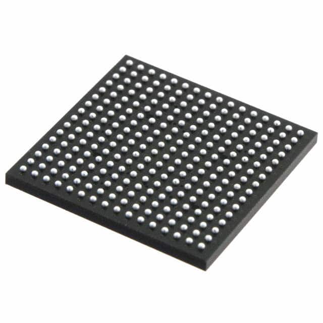
Semtech Corporation GN4121-CBE3
- Part No.:
- GN4121-CBE3
- Manufacturer:
- Semtech Corporation
- Category:
- Video Processing
- Package:
- 256-LBGA
- Datasheet:
-
GN4121-CBE3.pdf
- Description:
- IC VID PCI TO LOCAL BRDGE 256BGA
- Quantity:
- Payment:

- Shipping:

Inventory:3,313
Please send an inquiry. Send us your inquiry, and we will respond immediately.
Product details
Overview
GN4121-CBE3 from Gennum is a single-lane PCI Express 1.1 to local bus bridge IC designed as a companion for FPGA devices lacking on-chip PCIe SerDes. It integrates on-die PCIe PHY, link, and transaction layers; supports DDR SSTL local bus I/O up to 500 MB/s; provides FPGA bitstream loading over PCIe; and features live-on-power-up detection via on-chip Type 0 configuration space. It enables low-cost, high-performance bridging in FPGA-based embedded systems requiring PCIe connectivity.
For engineers reviewing the GN4121-CBE3 datasheet, pinout, applications, or equivalent options, this page delivers verified technical context, exact pin functions, real-world timing and power specs, FPGA interface design implications, and validated alternative options - all grounded in the official Gennum GN4121 Data Sheet (51539-0, June 2009).
Technical Context
The GN4121-CBE3 implements a hard-wired PCI Express Base Specification 1.1 x1 lane interface with integrated CML transmitter/receiver (PETp/PETn, PERp/PERn), full link and transaction layer logic, and a streamlined application layer supporting MSI and BAR access. Its local bus uses differential SSTL clocks (LCLK/LCLKn) and DDR data paths (P2L_DATA[15:0], L2P_DATA[15:0]) operating at up to 125 MHz DDR (250 MT/s), enabling 500 MB/s bidirectional throughput.
It embeds a 2-wire serial controller (SCLK/SDATA) for EEPROM-based boot configuration, a GPIO block (GPIO[15:0]) supporting interrupt routing, and an FPGA configuration loader (SPRI_CLK/SPRI_DATAOUT) enabling PCIe-hosted bitstream download and on-the-fly reconfiguration - all without consuming FPGA logic resources.
Key Specifications
| Parameter | Value and Actual Design Meaning |
|---|---|
| PCIe Compliance | PCI Express Base Specification 1.1, x1 lane, CML physical layer with 800–1200 mVpp differential output swing. |
| Local Bus Throughput | 500 MB/s bidirectional using 16-bit DDR SSTL I/O clocked at 125 MHz (250 MT/s), asynchronous to PCIe clock domain. |
| Power Consumption | 475–695 mW typical under PCIe x1 + 100 MHz local bus operation, with core supply at 1.2 V ±5% (VDDC/VDD_PCIE). |
| Configuration Space | On-chip Type 0 PCI configuration space with extended registers for power management, MSI, and PCIe capabilities - enables plug-and-play enumeration without FPGA activity. |
| FPGA Loader Interface | Dedicated Serial Programming Interface (SPRI) with SPRI_CLK, SPRI_DATAOUT, SPRI_CONFIG, SPRI_DONE - supports direct PCIe-hosted FPGA bitstream loading and dynamic reconfiguration. |
| Virtual Channel Support | One hardware virtual channel supporting all eight PCIe traffic classes, with VC_RDY output signaling DL_UP1 status for synchronous reset coordination. |
| I/O Voltage Levels | SSTL-18 for local bus (VCCO18 = 1.71–1.89 V), LVCMOS-3.3 for control/GPIO (VCCO33 = 3.0–3.6 V), and 1.2 V core (VDDC = 1.14–1.26 V). |
Pinout & Package
GN4121-CBE3 is housed in a 256-pin PBGA package (17 mm × 17 mm, 1.0 mm pitch) with exposed thermal pad. Pin assignments follow the documented ball map in Figure 2-1 of the datasheet, with dedicated power domains (VDDC, VCCO18, VCCO33, VDD_PCIE), PCIe CML lanes (PERp/PERn, PETp/PETn), differential local clocks (LCLK/LCLKn, P2L_CLKp/P2L_CLKn, L2P_CLKp/L2P_CLKn), and 16-bit DDR data buses (P2L_DATA[15:0], L2P_DATA[15:0]).
| Pin/Terminal | Circuit Role | Design Meaning |
|---|---|---|
| RSTIN | Global Asynchronous Reset Input | LVCMOS-3.3 active-low input initiating full device reset; required for system-level synchronization. |
| PETp / PETn | PCIe Transmit Differential Pair | CML outputs driving PCIe lane A; require AC coupling (150 nF) and 100 Ω differential termination per spec. |
| PERp / PERn | PCIe Receive Differential Pair | CML inputs receiving PCIe lane A; internally terminated, compatible with standard PCIe add-in card reference clocking. |
| LCLK / LCLKn | Local Bus Reference Clock Output | Differential SSTL-18 clock generated by internal PLL; drives FPGA source-synchronous receiver timing for inbound data (P2L_DATA). |
| L2P_DATA[15:0] | Local-to-PCIe Transmit Data Inputs | 16-bit SSTL-18 parallel inputs accepting outbound data from FPGA; sampled on rising/falling edges of L2P_CLKp/L2P_CLKn. |
| P2L_DATA[15:0] | PCIe-to-Local Receive Data Outputs | 16-bit SSTL-18 parallel outputs delivering inbound PCIe data to FPGA; valid relative to P2L_CLKp/P2L_CLKn edges. |
| SPRI_DATAOUT | FPGA Configuration Data Output | LVCMOS-3.3 bidirectional pin carrying bitstream data from GN4121-CBE3 to FPGA during PCIe-initiated configuration load. |
| GPIO[15:0] | General Purpose I/O | 16 configurable LVCMOS-3.3 pins usable for interrupt signaling, status monitoring, or control handshaking with FPGA or external logic. |
Key Features
| Feature | Design Value |
|---|---|
| No PCIe IP licensing required | Hard-wired PCIe PHY, link, and transaction layers eliminate FPGA resource usage and royalty costs associated with soft IP cores. |
| FPGA bitstream loader over PCIe | Enables host-initiated FPGA reconfiguration without external PROM, reducing BOM count and enabling field firmware upgrades. |
| Live-on-power-up enumeration | On-chip Type 0 configuration space allows BIOS auto-detection and enumeration before FPGA configuration - critical for boot-time PCIe device visibility. |
| Asynchronous local bus clocking | Local bus operates independently of PCIe clock rate, permitting dynamic frequency scaling and power optimization based on application bandwidth needs. |
| 2-wire serial boot interface | SCLK/SDATA pins support EEPROM-based default register loading (e.g., Subsystem Vendor ID, BAR sizes) at power-up, simplifying system initialization. |
Applications
| High-Speed FPGA-Based Data Acquisition | PCIe-Enabled Industrial Control Module |
|---|---|
Use Scenario: Real-time sensor data acquisition system using FPGA for preprocessing, with results streamed to host PC via PCIe. IC Role / Device Role / Timing Role: GN4121-CBE3 acts as PCIe endpoint bridge, handling protocol translation, DMA request arbitration, and clock domain crossing between PCIe root complex and FPGA logic. Use Value: Delivers deterministic 500 MB/s throughput using minimal FPGA resources, avoids PCIe IP licensing, and enables host-triggered FPGA reconfiguration for algorithm updates. | Use Scenario: Programmable logic controller (PLC) module integrating FPGA-based motion control logic with host supervision over PCIe. IC Role / Device Role / Timing Role: GN4121-CBE3 serves as local bus master interface, managing PCIe-to-FPGA command writes and FPGA-to-PCIe status reads while maintaining strict timing isolation via asynchronous clock domains. Use Value: Provides live-on-power-up device enumeration for immediate host visibility, supports GPIO-based interrupt signaling for event-driven control, and reduces system latency through dedicated DDR local bus I/O. |
| Embedded Vision Processing Node | Reconfigurable PCIe Add-in Card Platform |
Use Scenario: Camera interface board with FPGA performing image filtering and compression, feeding processed frames to host memory via PCIe. IC Role / Device Role / Timing Role: GN4121-CBE3 bridges PCIe transaction layer to FPGA's local bus, buffering inbound frame data and coordinating read/write transfers using P2L_VALID and L2P_RDY handshaking signals. Use Value: Achieves sustained 500 MB/s transfer using 16-bit DDR SSTL, supports payload sizes up to 512 bytes, and enables on-the-fly FPGA reconfiguration for switching between vision algorithms. | Use Scenario: Modular PCIe card platform where FPGA functionality is updated remotely via host software without physical access. IC Role / Device Role / Timing Role: GN4121-CBE3 functions as PCIe configuration loader and bridge controller, executing PCIe configuration space access and SPI-like bitstream delivery through SPRI interface. Use Value: Eliminates need for external configuration PROM, reduces PCB footprint and cost, and allows secure, authenticated firmware updates over existing PCIe infrastructure. |
Equivalent & Alternatives
The following parts are listed as comparable options for similar PCIe-to-local-bus bridging applications.
| Alternative Part | Technical Difference | Application Difference | Selection Advice |
|---|---|---|---|
| PLX Technology PEX8311 | PCI Express x1 to PCI/PCI-X bridge (not FPGA-optimized); requires external PCI clock and lacks integrated FPGA loader or DDR SSTL local bus. | Targets legacy PCI expansion, not FPGA-centric designs; no native support for on-the-fly FPGA reconfiguration. | Select when interfacing with PCI peripherals rather than FPGAs, and when PCIe-to-PCI protocol translation-not PCIe-to-FPGA bridging-is required. |
| Xilinx Virtex-5 FX series with PCIe LogiCORE | FPGA-integrated PCIe endpoint using soft IP; consumes significant FPGA logic, requires PCIe IP license, and lacks dedicated hardware loader interface. | Offers higher flexibility and multi-lane scalability but increases FPGA resource usage, power, and development complexity. | Select when full PCIe endpoint customization, multi-lane support, or integration with other FPGA logic is mandatory - not for cost-sensitive, low-resource FPGA companion use. |
Compared with PEX8311 and Virtex-5 FX, GN4121-CBE3 uniquely combines hardwired PCIe compliance, FPGA-optimized DDR SSTL local bus, and integrated bitstream loader - delivering lower BOM cost, reduced FPGA utilization, and simplified PCIe enablement for FPGA-based endpoints.
Availability
GN4121-CBE3 is available at Aetrix Electronics and suitable for high-speed FPGA interconnect, PCIe add-in card development, and industrial embedded systems requiring stable component supply and long-term lifecycle support.
Supply support for GN4121-CBE3 includes scheduled delivery planning, volume procurement assistance, BOM continuity management, traceable sourcing, and lifecycle availability coordination for OEM customers, industrial embedded developers, connected-device designers, and electronics production programs.
Manufacturer
Gennum Corporation was a Canadian semiconductor company specializing in high-speed serial interface solutions, acquired by Microchip Technology in 2012. It developed industry-leading PCIe bridge, video, and communications ICs before integration into Microchip's analog and interface portfolio.
The GN4121-CBE3 belongs to Gennum's GN412x family of PCIe bridge controllers, engineered specifically to offload PCIe protocol implementation from FPGAs - targeting cost-sensitive, high-performance embedded systems where SerDes-less FPGA devices require native PCIe connectivity.
FAQ
Does GN4121-CBE3 support PCIe 2.0 or higher?
No, GN4121-CBE3 complies strictly with PCI Express Base Specification 1.1. It implements a x1 lane CML PHY with 2.5 GT/s signaling and does not support PCIe 2.0 (5 GT/s) or later revisions. The datasheet (51539-0, June 2009) confirms 1.1 compliance, and no errata or revision documents extend this capability. GN4121-CBE3 remains a PCIe 1.1-only device.
What is the function of the SPRI interface on GN4121-CBE3?
The SPRI (Serial Programming Interface) on GN4121-CBE3 enables PCIe-hosted FPGA configuration loading. Pins SPRI_CLK, SPRI_DATAOUT, SPRI_CONFIG, SPRI_DONE, and SPRI_XI_SWAP form a dedicated interface that streams bitstream data from the GN4121-CBE3 to the attached FPGA. This eliminates external PROM and supports on-the-fly reconfiguration - a core differentiator of the GN4121-CBE3.
Can GN4121-CBE3 operate without an FPGA connected to its local bus?
No - GN4121-CBE3 requires an FPGA (or compatible logic device) on its local bus to function as intended. Its local interface (L2P_DATA, P2L_DATA, clocks, handshaking signals) is designed exclusively for FPGA attachment. While the device powers up "live" for enumeration, meaningful data transfer, configuration loading, and interrupt handling depend entirely on a properly interfaced FPGA.
What are the voltage requirements for GN4121-CBE3's I/O banks?
GN4121-CBE3 requires three distinct I/O supply voltages: VCCO18 = 1.71–1.89 V for SSTL-18 local bus signals (LCLK, P2L_DATA, L2P_DATA); VCCO33 = 3.0–3.6 V for LVCMOS-3.3 control/GPIO/2-wire pins (RSTIN, GPIO[15:0], SCLK, SDATA); and VREF = 833–969 mV (typically 900 mV) as reference for SSTL receivers. These are specified in Tables 3-2 and 3-5 of the datasheet.
Is GN4121-CBE3 pin-compatible with other members of the GN412x family?
GN4121-CBE3 is not pin-compatible with GN4122 or GN4124. Although all GN412x devices share the same 256-pin PBGA package outline, pin functions differ significantly across variants - particularly in PCIe lane count (x1 vs x4), local bus width, and feature set (e.g., GN4122 supports two virtual channels; GN4121 supports one). The datasheet confirms unique pin assignments per part number; substitution requires full schematic and layout review.
GN4121-CBE3 Specifications
- Product attributes
- Attribute value
- Manufacturer:
- Semtech Corporation
- Series:
- -
- Package/Case:
- 256-LBGA
- Packaging:
- Tray
- Product Status:
- Obsolete
- Function:
- -
- Applications:
- -
- Standards:
- -
- Control Interface:
- GPIO, I2C, PCIe
- Voltage - Supply:
- -
- Mounting Type:
- Surface Mount
- Grade:
- -
- Qualification:
- -
- Supplier Device Package:
- 256-BGA (17x17)
GN4121-CBE3 FAQ
1.How can I place an order for GN4121-CBE3 through Aetrix?
Please submit a Request for Quotation (RFQ) for GN4121-CBE3 on Aetrix. Our sales agent will provide a competitive quotation and guide you through the order confirmation once you accept the terms.
2.Are the price and stock information for GN4121-CBE3 reliable?
The price and inventory of GN4121-CBE3 are updated periodically and may fluctuate due to market conditions. Stock and pricing data are typically refreshed every 24 hours. Quotation validity for GN4121-CBE3 is usually 5 days.
3.What payment methods are accepted for GN4121-CBE3?
We accept Wire Transfer, PayPal, Credit Card, Western Union, MoneyGram, and Escrow for GN4121-CBE3 transactions.
Note: Certain payment methods may incur a processing fee.
4.How is shipping managed for GN4121-CBE3?
GN4121-CBE3 orders can be shipped via leading logistics carriers, including DHL, UPS, FedEx, TNT, or Registered Mail.
Once your GN4121-CBE3 order is processed, you will receive an email with the shipment details and tracking number.
Note: Tracking information may take up to 24 hours to appear. Express delivery typically takes 3–5 business days.
5.How can I obtain technical support or documentation for GN4121-CBE3?
For technical support, including GN4121-CBE3 datasheets, pinout diagrams, or application guidance, please contact our engineering support team. They can provide detailed documentation and assistance for your GN4121-CBE3 requirements.
6.How does Aetrix verify that GN4121-CBE3 is sourced from the original manufacturer or authorized distributors?
All GN4121-CBE3 products on Aetrix are procured from qualified distributors and authorized channels. Our dedicated quality assurance team conducts strict verification, including traceability checks and, if necessary, third-party testing. This ensures that GN4121-CBE3 meets industry standards.
7.What is the process for return or replacement of GN4121-CBE3?
All GN4121-CBE3 units undergo pre-shipment inspection (PSI). If there is an issue with GN4121-CBE3, returns or replacements are accepted under the following conditions:
1.Quantity discrepancies, incorrect items, or visible external defects (such as breakage or corrosion), acknowledged by Aetrix.
2.The issue is reported within 90 days of delivery.
3.The GN4121-CBE3 part is unused and in its original packaging.
Return procedure for GN4121-CBE3:
1.Submit a request within 90 days.
2.Obtain a Return Material Authorization (RMA) from Aetrix.
GN4121-CBE3 Tags

-
HDMI2C1-6C1
STMicroelectronics

-
ADA4430-1YKSZ-R7
Analog Devices Inc.

-
LM1881MX/NOPB
Texas Instruments

-
SN75DP130SSRGZR
Texas Instruments

-
EQCO30T5.2
Microchip Technology

-
LMH1980MM/NOPB
Texas Instruments

-
EQCO30R5.D
Microchip Technology

-
SII9022ACNU
Lattice Semiconductor Corporation

-
SN65DP159RGZR
Texas Instruments

-
SN65DP159RSBR
Texas Instruments

-
SN65DP141RLJR
Texas Instruments

-
LMH0303SQ/NOPB
Texas Instruments
Tech Hub

Comparator circuit design covering voltage thresholds, input limits, open-collector outputs, LM393 wiring, op-amp differences, hysteresis, timing, window detection and practical fault diagnosis.
Schmitt triggers use separate rising and falling thresholds to stabilize slow or noisy signals. This guide covers hysteresis, 74HC14 and 74HCT14 selection, comparator calculations, RC oscillators and p…
Counterfeit components can hide behind convincing markings and passing basic function tests. This engineering reference covers source traceability, external inspection, X-ray, XRF, electrical testing, …
A practical engineering and sourcing framework covering lifecycle verification, lifetime-buy calculations, replacement qualification, supplier checks and counterfeit-risk controls.
TTL and CMOS logic families differ in thresholds, loading, output drive, power and timing. This engineering guide compares 74HC and 74HCT, calculates noise margins and checks 3.3 V/5 V compatibility.
A practical engineering guide to 3.3V and 5V logic compatibility, input thresholds, resistor dividers, translator ICs, MOSFET level shifting, I2C pull-ups, timing limits and power-sequencing risks.
The 74HC595 uses push-pull logic outputs, while the TPIC6B595 uses 50 V open-drain DMOS sinks for higher-power loads. This guide compares timing, current limits, 3.3 V interfacing, load wiring, thermal…
The 74HC595 converts serial data into eight stable parallel outputs. This guide covers pin functions, shift and storage timing, OE and MR behavior, drive-current limits, cascading, voltage compatibilit…
A technical comparison of level-sensitive latches and edge-triggered flip-flops, covering timing windows, setup and hold limits, master–slave operation, time borrowing, race-through, HDL inference and…
A D latch stores one bit while Enable controls when data can pass. This reference covers gate-level operation, truth tables, transparency, setup and hold timing, LE versus OE, common ICs and practical …