Send an Inquiry

To receive a quote for your project, please fill in the following information, and we’ll get back to you promptly.

Name*
Company*
Email Address*
Phone/WhatsApp
Part Number*
Quantity*
Message
Submit Inventory List

Please fill in the following information, and we’ll get back to you promptly.

Name*
Company*
Email Address*
Phone/WhatsApp
Upload My List
Message

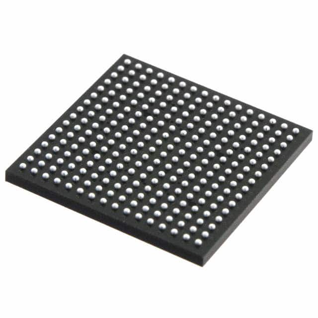
Semtech Corporation GN4124-CBE3

Part No.:
GN4124-CBE3
Manufacturer:
Semtech Corporation
Category:
Video Processing
Package:
256-LBGA
Datasheet:
AetrixGN4124-CBE3.pdf
Description:
IC VID PCI TO LOCAL BRDGE 256BGA
Quantity:
Payment:
Payment
Shipping:
Shipping

Inventory:1,608

Please send an inquiry. Send us your inquiry, and we will respond immediately.

Part Number
Quantity*
Price
Name*
Company
Email*
Comments

Product details

Overview

GN4124-CBE3 from Gennum is a 4-lane PCI Express to local bus bridge IC designed as an FPGA companion for high-performance native PCIe bridging in embedded and industrial systems. It integrates on-chip PCIe PHY, link, and transaction layers compliant with PCI Express Base Specification 1.1; supports dual virtual channels; delivers up to 800 MB/s bidirectional throughput via DDR SSTL local bus; and enables FPGA bitstream loading over PCIe.

For engineers reviewing the GN4124-CBE3 datasheet, pinout, applications, or equivalent options, key selection considerations include PCIe x4 lane compliance, DDR SSTL local bus timing (200 MHz DDR clock), dual VC support, on-the-fly FPGA configuration capability, and integrated MSI interrupt generation without external IP licensing.

Technical Context

The GN4124-CBE3 implements a hardwired PCI Express 1.1 stack-including physical, data link, and transaction layers-eliminating the need for licensed PCIe IP in FPGA-based designs. Its local bus interface uses source-synchronous DDR SSTL signaling (1.8 V) with separate SDR control clocks and DDR data clocks, enabling asynchronous operation relative to PCIe reference clocking.

It features a dedicated FPGA configuration loader supporting serial programming over PCIe, a 2-wire (I²C-compatible) controller for EEPROM boot and register access, and a flexible interrupt controller routing GPIO or internal sources to MSI or GPIO pins. Virtual channel arbitration uses independent on-chip buffering per VC to prevent blocking between traffic classes.

Key Specifications

Parameter Value and Actual Design Meaning
PCI Express InterfaceCompliant with PCI Express Base Specification 1.1, x4 lane configuration, CML I/O, 2.5 GT/s data rate
Local Bus ThroughputUp to 800 MB/s bidirectional using 16-bit DDR SSTL at 200 MHz DDR clock (400 MT/s)
Virtual ChannelsTwo independent hardware virtual channels with separate buffering and non-blocking arbitration
FPGA Configuration SupportOn-chip serial programming interface (SPRI) enables PCIe-hosted bitstream loading and on-the-fly reconfiguration
Power Supply Requirements1.2 V core (VDDC/VDD_PCIE/VDDAUX/PLL_AVDD), 1.8 V I/O (VCCO18), 3.3 V LVCMOS (VCCO33/VDDW/VDDP), 900 mV VREF
Operating Temperature0 °C to +85 °C ambient, validated for industrial-grade embedded applications
Interrupt CapabilityMessage Signaled Interrupts (MSI) generated from GPIO or internal sources; configurable routing to up to four GPIO pins

Pinout & Package

GN4124-CBE3 is housed in a 256-pin PBGA package (17 mm × 17 mm, 1.0 mm pitch) with exposed thermal pad. Pin assignments are optimized for PCIe lane routing, DDR SSTL local bus signal integrity, and FPGA co-location.

Pin/Terminal Circuit Role Design Meaning
P2L_DATA[15:0]PCIe-to-Local Receive Data Output16-bit DDR SSTL output carrying inbound PCIe payload to FPGA; synchronized to P2L_CLKp/n
L2P_DATA[15:0]Local-to-PCIe Transmit Data Input16-bit DDR SSTL input accepting outbound FPGA data; referenced to L2P_CLKp/n with ODT enabled
P2L_CLKp / P2L_CLKnReceiver Source-Synchronous Clock OutputDifferential 1.8 V SSTL clock driving FPGA capture of P2L_DATA; phase-aligned to data valid window
L2P_CLKp / L2P_CLKnTransmitter Source-Synchronous Clock InputDifferential 1.8 V SSTL clock from FPGA controlling L2P_DATA timing; requires external ODT termination
PERp[3:0] / PERn[3:0]PCIe Receive Input (x4 lanes)CML differential inputs accepting PCIe upstream traffic; polarity inversion auto-detected during link training
PETp[3:0] / PETn[3:0]PCIe Transmit Output (x4 lanes)CML differential outputs driving PCIe downstream traffic; terminated via VTT_AB/VTT_CD at 1.5 V
GPIO[15:0]General Purpose I/O16× 3.3 V LVCMOS bidirectional pins supporting interrupt routing, status monitoring, or control signaling
SCLK / SDATA2-Wire Serial InterfaceI²C-compatible master/target interface for EEPROM boot configuration and runtime register access

Key Features

Feature Design Value
Hardwired PCIe 1.1 StackEliminates FPGA resource usage and PCIe IP licensing cost; reduces design risk and time-to-market
DDR SSTL Local BusEnables 800 MB/s bandwidth with minimal pin count (32 pins for 16-bit DDR + clocks) and low-power operation
Live-on-Power-Up OperationOn-chip Type 0 PCI configuration space allows BIOS enumeration before FPGA configuration, enabling plug-and-play system boot
FPGA Bitstream LoaderSupports PCIe-hosted FPGA configuration and dynamic reconfiguration without external PROM or JTAG dependency
Dual Virtual Channel ArbitrationPrevents latency-sensitive traffic (e.g., real-time sync) from being blocked by high-bandwidth streams (e.g., video DMA)
Integrated 2-Wire ControllerLoads default register values (BAR sizes, subsystem IDs) from EEPROM at reset; also serves as runtime register access port

Applications

Medical Imaging Acquisition Industrial Machine Vision

Use Scenario: High-speed raw image data transfer from FPGA-accelerated image sensor interface to host memory via PCIe.

IC Role / Device Role / Timing Role: GN4124-CBE3 acts as PCIe-to-local bus bridge, receiving pixel data over DDR SSTL from FPGA and forwarding it upstream as PCIe TLPs.

Use Value: 800 MB/s sustained throughput meets real-time 12-bit 4K@60fps acquisition; dual VC isolates control commands from streaming data.

Use Scenario: FPGA-based preprocessing pipeline (demosaic, HDR merge) feeding results to host PC for AI inference.

IC Role / Device Role / Timing Role: GN4124-CBE3 provides local bus interface for FPGA to initiate PCIe master reads/writes to host DRAM while maintaining low-latency response to trigger signals.

Use Value: Asynchronous local bus clocking allows FPGA logic to run at optimal frequency independent of PCIe link rate; SPRI enables field-upgradable vision firmware.

Test & Measurement Equipment Communications Protocol Analyzer

Use Scenario: Digitizer card capturing multi-channel analog waveforms at 1 GS/s, buffering in FPGA, then streaming to host via PCIe.

IC Role / Device Role / Timing Role: GN4124-CBE3 serves as PCIe endpoint, managing DMA transfers from FPGA memory buffers using MSI interrupts for completion notification.

Use Value: On-chip MSI controller eliminates discrete interrupt logic; live-on-power-up ensures immediate BIOS detection without FPGA boot delay.

Use Scenario: Protocol analyzer capturing PCIe, SATA, or USB traffic and correlating timestamps across interfaces using FPGA logic.

IC Role / Device Role / Timing Role: GN4124-CBE3 bridges FPGA-based packet parser to host for storage and analysis; 2-wire interface loads unique device identifiers from EEPROM.

Use Value: Dual VC separates timestamp metadata (VC0) from payload data (VC1), guaranteeing sub-microsecond latency for time-critical events.

Equivalent & Alternatives

The following parts are listed as comparable options for similar PCIe-to-FPGA bridging applications.

Alternative Part Technical Difference Application Difference Selection Advice
Xilinx Virtex-5 FX70T (with PCIe LogiCORE)Integrates PCIe hard IP but consumes significant FPGA fabric; requires PCIe IP license and complex timing closureBetter suited for highly integrated SoC-like designs where PCIe endpoint and application logic share same dieChoose when maximum integration and deterministic latency outweigh cost, power, and design complexity trade-offs
PLX Technology PEX 8311PCI Express-to-PCI-X bridge; lacks FPGA-optimized local bus, no DDR SSTL, no on-chip FPGA loader or VC supportTargets legacy PCI-X peripheral expansion, not FPGA co-processing or reconfigurable accelerationChoose only for backward compatibility with existing PCI-X infrastructure; not a functional substitute for GN4124-CBE3's FPGA-centric architecture

Compared with Xilinx Virtex-5 FX70T, GN4124-CBE3 offloads PCIe protocol handling entirely, freeing FPGA resources for application logic and reducing power by ~300 mW; compared with PLX PEX8311, GN4124-CBE3 provides purpose-built DDR SSTL interface, dual VC arbitration, and PCIe-hosted FPGA configuration-enabling agile, low-footprint reconfigurable systems.

Availability

GN4124-CBE3 is available at Aetrix Electronics and suitable for medical imaging acquisition, industrial machine vision, test & measurement equipment, communications protocol analyzers, and FPGA-based accelerator cards requiring stable component supply and long-term industrial lifecycle support.

Supply support for GN4124-CBE3 includes scheduled delivery planning, volume procurement assistance, BOM continuity management, traceable sourcing, and lifecycle availability coordination for OEM customers, industrial embedded developers, connected-device designers, and electronics production programs.

Manufacturer

Gennum Corporation was a Canadian semiconductor company specializing in high-speed serial interface solutions, acquired by Microsemi in 2011. Its products targeted demanding embedded, broadcast, and industrial applications.

The GN4124-CBE3 belongs to Gennum's PCI Express Bridge Controller family, engineered specifically to enable cost-effective, low-power, FPGA-centric PCIe endpoint designs without requiring licensed protocol IP or complex FPGA resource allocation.

FAQ

Does GN4124-CBE3 support PCIe 2.0 or higher?

No, GN4124-CBE3 is compliant only with PCI Express Base Specification 1.1 (2.5 GT/s). It does not support PCIe 2.0 (5.0 GT/s) or later generations. The device's PHY, link, and transaction layers are fixed-function and not upgradeable via firmware or configuration. For PCIe 2.0+ requirements, alternative bridge solutions must be evaluated.

What is the role of the SPRI interface in GN4124-CBE3?

The Serial Programming Interface (SPRI) in GN4124-CBE3 enables PCIe-hosted FPGA configuration: the host CPU writes bitstream data to GN4124-CBE3's SPRI registers over BAR4, and GN4124-CBE3 serially clocks it out to the attached FPGA. This eliminates external PROM and supports on-the-fly reconfiguration-critical for field-upgradable GN4124-CBE3-based systems.

Can GN4124-CBE3 operate with a local bus clock slower than 200 MHz?

Yes, GN4124-CBE3 supports asynchronous local bus operation at frequencies below 200 MHz. The local bus clock (LCLK/LCLKn) may be scaled down to match FPGA logic requirements, reducing dynamic power consumption. Minimum supported rate is determined by setup/hold timing margins in the target FPGA I/O bank-not by GN4124-CBE3 itself.

How does GN4124-CBE3 handle PCIe link training with polarity inversion?

GN4124-CBE3 automatically detects and compensates for inverted polarity on PCIe receive lanes (PERp[3:0]/PERn[3:0]) during link training. This allows PCB layout flexibility-such as avoiding signal crossovers-without requiring manual lane swapping or strap configuration. The feature is implemented in the hardwired PHY and requires no user intervention or register programming in GN4124-CBE3.

Is GN4124-CBE3 pin-compatible with GN4121?

No, GN4124-CBE3 is not pin-compatible with GN4121. While both belong to the same Gennum family and share architectural similarities, GN4121 is a x1-lane PCIe bridge with different pin count, ball map, and I/O assignment. The GN4124-CBE3 uses a 256-ball PBGA package optimized for x4 lane routing and higher local bus bandwidth, whereas GN4121 uses a smaller package with reduced lane and I/O count.

GN4124-CBE3 Specifications

Product attributes
Attribute value
Manufacturer:
Semtech Corporation
Series:
-
Package/Case:
256-LBGA
Packaging:
Tray
Product Status:
Obsolete
Function:
-
Applications:
-
Standards:
-
Control Interface:
-
Voltage - Supply:
-
Mounting Type:
Surface Mount
Grade:
-
Qualification:
-
Supplier Device Package:
256-BGA (17x17)

GN4124-CBE3 FAQ

1.How can I place an order for GN4124-CBE3 through Aetrix?

Please submit a Request for Quotation (RFQ) for GN4124-CBE3 on Aetrix. Our sales agent will provide a competitive quotation and guide you through the order confirmation once you accept the terms.

2.Are the price and stock information for GN4124-CBE3 reliable?

The price and inventory of GN4124-CBE3 are updated periodically and may fluctuate due to market conditions. Stock and pricing data are typically refreshed every 24 hours. Quotation validity for GN4124-CBE3 is usually 5 days.

3.What payment methods are accepted for GN4124-CBE3?

We accept Wire Transfer, PayPal, Credit Card, Western Union, MoneyGram, and Escrow for GN4124-CBE3 transactions.

Note: Certain payment methods may incur a processing fee.

4.How is shipping managed for GN4124-CBE3?

GN4124-CBE3 orders can be shipped via leading logistics carriers, including DHL, UPS, FedEx, TNT, or Registered Mail.

Once your GN4124-CBE3 order is processed, you will receive an email with the shipment details and tracking number.

Note: Tracking information may take up to 24 hours to appear. Express delivery typically takes 3–5 business days.

5.How can I obtain technical support or documentation for GN4124-CBE3?

For technical support, including GN4124-CBE3 datasheets, pinout diagrams, or application guidance, please contact our engineering support team. They can provide detailed documentation and assistance for your GN4124-CBE3 requirements.

6.How does Aetrix verify that GN4124-CBE3 is sourced from the original manufacturer or authorized distributors?

All GN4124-CBE3 products on Aetrix are procured from qualified distributors and authorized channels. Our dedicated quality assurance team conducts strict verification, including traceability checks and, if necessary, third-party testing. This ensures that GN4124-CBE3 meets industry standards.

7.What is the process for return or replacement of GN4124-CBE3?

All GN4124-CBE3 units undergo pre-shipment inspection (PSI). If there is an issue with GN4124-CBE3, returns or replacements are accepted under the following conditions:

1.Quantity discrepancies, incorrect items, or visible external defects (such as breakage or corrosion), acknowledged by Aetrix.

2.The issue is reported within 90 days of delivery.

3.The GN4124-CBE3 part is unused and in its original packaging.

Return procedure for GN4124-CBE3:

1.Submit a request within 90 days.

2.Obtain a Return Material Authorization (RMA) from Aetrix.

GN4124-CBE3 Tags

  • GN4124-CBE3
  • GN4124-CBE3 PDF
  • GN4124-CBE3 Datasheet
  • GN4124-CBE3 Specifications
  • GN4124-CBE3 Images
  • Semtech Corporation
  • Semtech Corporation GN4124-CBE3
  • Buy GN4124-CBE3
  • GN4124-CBE3 Price
  • GN4124-CBE3 Distributor
  • GN4124-CBE3 Supplier
  • GN4124-CBE3 Wholesale
Related Products
HDMI2C1-6C1
HDMI2C1-6C1

STMicroelectronics

ADA4430-1YKSZ-R7
ADA4430-1YKSZ-R7

Analog Devices Inc.

LM1881MX/NOPB
LM1881MX/NOPB

Texas Instruments

SN75DP130SSRGZR
SN75DP130SSRGZR

Texas Instruments

EQCO30T5.2
EQCO30T5.2

Microchip Technology

LMH1980MM/NOPB
LMH1980MM/NOPB

Texas Instruments

EQCO30R5.D
EQCO30R5.D

Microchip Technology

SII9022ACNU
SII9022ACNU

Lattice Semiconductor Corporation

SN65DP159RGZR
SN65DP159RGZR

Texas Instruments

SN65DP159RSBR
SN65DP159RSBR

Texas Instruments

SN65DP141RLJR
SN65DP141RLJR

Texas Instruments

LMH0303SQ/NOPB
LMH0303SQ/NOPB

Texas Instruments

Tech Hub

Search

Search

PRODUCT

PRODUCT

PHONE

PHONE

USER

USER