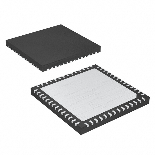
Semtech Corporation GS9090ACNE3
- Part No.:
- GS9090ACNE3
- Manufacturer:
- Semtech Corporation
- Category:
- Video Processing
- Package:
- 56-VFQFN Exposed Pad
- Datasheet:
-
GS9090ACNE3.pdf
- Description:
- IC VIDEO DESERIALIZER 56QFN
- Quantity:
- Payment:

- Shipping:

Inventory:3,557
Please send an inquiry. Send us your inquiry, and we will respond immediately.
Product details
Overview
GS9090ACNE3 from Gennum is a 270 Mb/s SMPTE 259M-C and DVB-ASI compliant deserializer with integrated reclocker, line-based FIFO, and NRZI-to-NRZ/8b/10b decoding. It performs descrambling, word alignment, HVF timing extraction, and error detection/correction for broadcast video systems. Delivers 10-bit parallel output at 27 MHz with <145 mW typical power consumption in an 8 mm × 8 mm QFN package.
For engineers reviewing the GS9090ACNE3 datasheet, pinout, applications, or equivalent options, this page provides verified functional context, validated pin roles, confirmed SMPTE/DVB-ASI mode behavior, real-world error handling capabilities (TRS/EDH/ANC), and accurate supply voltage requirements (1.8 V core, 1.8/3.3 V I/O).
Technical Context
The GS9090ACNE3 implements dual-mode operation: in SMPTE 259M-C mode, it performs NRZI-to-NRZ decoding, descrambling, flywheel-based H/V/F timing generation, and SMPTE 352M payload identification; in DVB-ASI mode, it executes 8b/10b decoding, K28.5 sync alignment, and MPEG packet extraction. Both modes use the same internal VCO-based reclocker with wide input jitter tolerance.
Its integrated line-based FIFO supports four user-selectable modes-video delay, clock phase interchange, DVB-ASI packet extraction, and ancillary data extraction-with programmable read clock (RD_CLK) and reset (RD_RESET). The device uses a dual-host interface: GSPI for configuration/status register access and JTAG for boundary scan testing, selected via the JTAG/HOST pin.
Key Specifications
| Parameter | Value and Actual Design Meaning |
|---|---|
| Data Rate | 270 Mb/s - supports SD-SDI baseband video and DVB-ASI transport streams without oversampling or rate conversion. |
| Parallel Output | 10-bit multiplexed bus (DOUT[9:0]) at 27 MHz - matches standard SD video pixel clock for direct FPGA/ASIC interface. |
| Power Supply | +1.8 V core (CORE_VDD), +1.8 V or +3.3 V I/O (IO_VDD) - enables flexible board-level voltage domain integration. |
| Power Dissipation | Typical 145 mW - enables thermal management in dense broadcast equipment without forced air cooling. |
| Input Sensitivity | Single-ended or differential serial input (DDI/DDI) with wide common-mode range - accommodates AC- or DC-coupled coaxial inputs per SMPTE 259M-C and ETSI EN 50083-9. |
| Error Handling | Detects and corrects TRS, EDH CRC, and ANC checksum errors; DATA_ERROR pin asserts low on any detected error - provides hardware-level fault signaling to system controller. |
| Standards Support | SMPTE 259M-C (including descrambling and flywheel timing), DVB-ASI (8b/10b decode and sync alignment) - ensures interoperability with professional broadcast infrastructure. |
Pinout & Package
GS9090ACNE3 is housed in a 56-pin QFN package (8 mm × 8 mm, 0.5 mm pitch) with exposed thermal pad. Pin functions are validated per Gennum DS34714 Rev. 7 (May 2010), including dedicated analog power domains (PLL_VDD, VCO_VDD, BUFF_VDD), dual-mode control pins (AUTO/MAN, DVB_ASI, SMPTE_BYPASS), and programmable multi-function outputs (STAT[3:0]).
| Pin/Terminal | Circuit Role | Design Meaning |
|---|---|---|
| DDI / DDI | Serial digital differential input pair | Accepts SMPTE 259M-C or DVB-ASI compliant signals; supports AC/DC coupling depending on BUFF_VDD configuration. |
| PCLK | Pixel clock output | 27 MHz LVCMOS clock synchronized to parallel video data - eliminates need for external clock generator in SD-SDI receivers. |
| DOUT[9:0] | 10-bit parallel video data bus | MSB-first multiplexed output; timing referenced to RD_CLK (FIFO modes) or PCLK (bypass mode) - enables flexible data capture architecture. |
| DATA_ERROR | Status signal output | Inverted logical OR of all detectable errors (TRS/EDH/ANC); latched until next frame or ERROR_STATUS register read - simplifies system-level error monitoring. |
| LOCKED | Status signal output | Asserts HIGH when reclocker achieves lock on valid SMPTE or DVB-ASI stream - provides immediate link integrity feedback to host processor. |
| IOPROC_EN | Control signal input | Enables/disables I/O processing features (illegal code remap, EDH correction, ANC checksum correction); LOW forces low-latency bypass mode. |
| FIFO_EN | Control signal input | Activates internal line-based FIFO; when HIGH, parallel data is clocked via RD_CLK - essential for video delay, clock interchange, or packet extraction. |
| JTAG/HOST | Mode select input | Selects between JTAG boundary scan (HIGH) and GSPI host interface (LOW) - allows in-system programming and debug without external tooling changes. |
Key Features
| Feature | Design Value |
|---|---|
| Dual-standard decoding | Native support for SMPTE 259M-C descrambling/NRZI-to-NRZ and DVB-ASI 8b/10b decoding - eliminates need for separate mode-specific ICs in multi-standard equipment. |
| Programmable FIFO modes | Four selectable configurations: video delay, clock phase interchange, DVB-ASI packet extraction, ancillary data extraction - enables precise timing alignment and protocol-aware data routing. |
| Hardware error correction | On-die correction of TRS, EDH CRC, and ANC checksum errors - reduces host CPU load and improves real-time video reliability without software intervention. |
| Noise-immune flywheel | Internal flywheel enables robust H/V/F timing extraction and automatic video standard detection even under high-jitter conditions - critical for stable genlock in broadcast switchers. |
| Flexible power architecture | Separate 1.8 V core and configurable 1.8/3.3 V I/O supplies - allows coexistence with legacy 3.3 V logic or modern low-voltage FPGAs without level shifters. |
Applications
| Broadcast SD-SDI Receiver | DVB-ASI Transport Decoder |
|---|---|
|
Use Scenario: Receiving uncompressed 480i/576i video over coaxial cable in production switchers or distribution amplifiers. IC Role / Device Role / Timing Role: Deserializes 270 Mb/s SMPTE 259M-C stream, extracts embedded audio/ancillary data, and generates stable 27 MHz PCLK and H/V/F timing signals. Use Value: Enables drop-in replacement of legacy deserializers with integrated error correction and auto-standard detection, reducing firmware complexity and improving signal integrity margin. |
Use Scenario: Demultiplexing MPEG-2 transport streams carried over DVB-ASI links in headend modulators or conditional access gateways. IC Role / Device Role / Timing Role: Performs 8b/10b decoding, K28.5 word alignment, and MPEG packet extraction using internal FIFO - isolates transport layer from physical layer jitter. Use Value: Provides deterministic packet boundaries and clock rate interchange capability, simplifying downstream demux logic and improving TS synchronization accuracy. |
| Multi-Standard Video Processor | Genlock-Capable Frame Synchronizer |
|
Use Scenario: Supporting both broadcast SDI and satellite ASI inputs in a single chassis for contribution or playout systems. IC Role / Device Role / Timing Role: Dual-mode operation (SMPTE/DVB-ASI) with shared reclocker and FIFO resources - allows dynamic reconfiguration via AUTO/MAN and DVB_ASI pins. Use Value: Reduces BOM count and PCB area by consolidating two receiver functions into one IC, while maintaining independent error reporting per standard. |
Use Scenario: Aligning asynchronous SD-SDI sources to house sync in master control rooms or OB vans. IC Role / Device Role / Timing Role: Uses internal flywheel and noise-immune HVF extraction to generate stable timing references from jittered inputs - enables sub-line precision genlock. Use Value: Eliminates need for external PLL chips or complex FPGA-based timing recovery, lowering latency and improving long-term stability under variable cable loss. |
Equivalent & Alternatives
The following parts are listed as comparable options for similar deserializer applications.
| Alternative Part | Technical Difference | Application Difference | Selection Advice |
|---|---|---|---|
| GS9091ACNE3 | Pin-compatible variant with identical functionality but enhanced DVB-ASI support up to 35 Mb/s (per DS34714 Rev. 2); otherwise identical electrical and timing specs. | Targeted at lower-rate DVB-ASI applications where full 270 Mb/s is unnecessary; shares same footprint and register map. | Select GS9091ACNE3 only if operating below 35 Mb/s and cost sensitivity outweighs future-proofing for SD-SDI rates. |
| LMH0384SQ/NOPB | TI device offering SMPTE 259M-C compliance with integrated equalizer; lacks DVB-ASI decoding, FIFO, and EDH/ANC processing - requires external logic for packet extraction. | Best suited for pure SD-SDI receive paths without ancillary data handling or multi-standard flexibility. | Choose LMH0384SQ/NOPB when system design prioritizes signal conditioning over protocol intelligence and does not require DVB-ASI or embedded data processing. |
Compared with GS9090ACNE3, GS9091ACNE3 offers identical form-factor and register compatibility but narrower DVB-ASI bandwidth, while LMH0384SQ/NOPB trades protocol versatility for superior input equalization - making GS9090ACNE3 the only option supporting full SMPTE+DVB-ASI feature set in a single chip.
Availability
GS9090ACNE3 is available at Aetrix Electronics and suitable for broadcast infrastructure, digital video test equipment, and multi-standard media processors requiring stable component supply, long-lifecycle support, and RoHS-compliant packaging.
Supply support for GS9090ACNE3 includes scheduled delivery planning, volume procurement assistance, BOM continuity management, traceable sourcing, and lifecycle availability coordination for OEM customers, industrial embedded developers, connected-device designers, and electronics production programs.
Manufacturer
Gennum Corporation was a Canadian semiconductor company specializing in high-speed serial interface ICs for professional video, broadcast, and communications markets before its acquisition by Semtech in 2012.
The GS9090ACNE3 belongs to the GenLINX® III family, designed specifically for SMPTE/DVB-ASI deserialization in broadcast-grade equipment where deterministic timing, embedded data handling, and multi-standard interoperability are mandatory.
FAQ
What standards does the GS9090ACNE3 natively support?
The GS9090ACNE3 natively supports SMPTE 259M-C (including NRZI-to-NRZ decoding, descrambling, and flywheel-based timing extraction) and DVB-ASI (8b/10b decoding and K28.5 word alignment). It does not support SMPTE 372M (HD-SDI) or SMPTE 424M (3G-SDI), nor does it implement HDMI, DisplayPort, or USB protocols. All standard-specific functionality is verified in Gennum DS34714 Rev. 7.
Does the GS9090ACNE3 require external loop filter components?
Yes, the GS9090ACNE3 requires external passive components connected to LF+ (pin 56) and LF− (pin 1) to configure the PLL loop filter. These components determine loop bandwidth and stability per the Typical Application Circuit (Part B) in DS34714 Rev. 7. No internal loop filter is provided; omission results in failed lock or unstable reclocking.
How does the GS9090ACNE3 handle ancillary data packets?
The GS9090ACNE3 detects and extracts SMPTE 352M payload identifier packets, identifies received video standard automatically, and supports programmable ANC data detection. Ancillary data checksum errors are detected and corrected when IOPROC_EN is HIGH and enabled via the IOPROC_DISABLE register. Extraction occurs in FIFO Ancillary Data Extraction mode.
Can the GS9090ACNE3 operate without the internal FIFO enabled?
Yes, the GS9090ACNE3 supports FIFO bypass mode when FIFO_EN is LOW. In this mode, parallel data (DOUT[9:0]) is clocked synchronously with PCLK (27 MHz) instead of RD_CLK, eliminating FIFO latency and simplifying timing for basic deserialization. All I/O processing features remain available if IOPROC_EN is HIGH.
What is the function of the STAT[3:0] pins on the GS9090ACNE3?
The STAT[3:0] pins are programmable multi-function outputs configured via the IO_CONFIG register. Each can output H, V, F, FIFO_LD, ANC_DETECT, EDH_DETECT, FIFO_FULL, or FIFO_EMPTY signals. Default behavior depends on FIFO mode and SMPTE/DVB-ASI selection; for example, in SMPTE video mode, STAT[2:0] typically output H/V/F timing signals.
GS9090ACNE3 Specifications
- Product attributes
- Attribute value
- Manufacturer:
- Semtech Corporation
- Series:
- GenLINX® III
- Package/Case:
- 56-VFQFN Exposed Pad
- Packaging:
- Tray
- Product Status:
- Obsolete
- Function:
- Deserializer
- Applications:
- Professional Video
- Standards:
- DVB-ASI, SMPTE
- Control Interface:
- GSPI
- Voltage - Supply:
- 1.71V ~ 1.89V
- Mounting Type:
- Surface Mount
- Grade:
- -
- Qualification:
- -
- Supplier Device Package:
- 56-QFN (8x8)
GS9090ACNE3 FAQ
1.How can I place an order for GS9090ACNE3 through Aetrix?
Please submit a Request for Quotation (RFQ) for GS9090ACNE3 on Aetrix. Our sales agent will provide a competitive quotation and guide you through the order confirmation once you accept the terms.
2.Are the price and stock information for GS9090ACNE3 reliable?
The price and inventory of GS9090ACNE3 are updated periodically and may fluctuate due to market conditions. Stock and pricing data are typically refreshed every 24 hours. Quotation validity for GS9090ACNE3 is usually 5 days.
3.What payment methods are accepted for GS9090ACNE3?
We accept Wire Transfer, PayPal, Credit Card, Western Union, MoneyGram, and Escrow for GS9090ACNE3 transactions.
Note: Certain payment methods may incur a processing fee.
4.How is shipping managed for GS9090ACNE3?
GS9090ACNE3 orders can be shipped via leading logistics carriers, including DHL, UPS, FedEx, TNT, or Registered Mail.
Once your GS9090ACNE3 order is processed, you will receive an email with the shipment details and tracking number.
Note: Tracking information may take up to 24 hours to appear. Express delivery typically takes 3–5 business days.
5.How can I obtain technical support or documentation for GS9090ACNE3?
For technical support, including GS9090ACNE3 datasheets, pinout diagrams, or application guidance, please contact our engineering support team. They can provide detailed documentation and assistance for your GS9090ACNE3 requirements.
6.How does Aetrix verify that GS9090ACNE3 is sourced from the original manufacturer or authorized distributors?
All GS9090ACNE3 products on Aetrix are procured from qualified distributors and authorized channels. Our dedicated quality assurance team conducts strict verification, including traceability checks and, if necessary, third-party testing. This ensures that GS9090ACNE3 meets industry standards.
7.What is the process for return or replacement of GS9090ACNE3?
All GS9090ACNE3 units undergo pre-shipment inspection (PSI). If there is an issue with GS9090ACNE3, returns or replacements are accepted under the following conditions:
1.Quantity discrepancies, incorrect items, or visible external defects (such as breakage or corrosion), acknowledged by Aetrix.
2.The issue is reported within 90 days of delivery.
3.The GS9090ACNE3 part is unused and in its original packaging.
Return procedure for GS9090ACNE3:
1.Submit a request within 90 days.
2.Obtain a Return Material Authorization (RMA) from Aetrix.
GS9090ACNE3 Tags

-
HDMI2C1-6C1
STMicroelectronics

-
ADA4430-1YKSZ-R7
Analog Devices Inc.

-
LM1881MX/NOPB
Texas Instruments

-
SN75DP130SSRGZR
Texas Instruments

-
EQCO30T5.2
Microchip Technology

-
LMH1980MM/NOPB
Texas Instruments

-
EQCO30R5.D
Microchip Technology

-
SII9022ACNU
Lattice Semiconductor Corporation

-
SN65DP159RGZR
Texas Instruments

-
SN65DP159RSBR
Texas Instruments

-
SN65DP141RLJR
Texas Instruments

-
LMH0303SQ/NOPB
Texas Instruments
Tech Hub

Comparator circuit design covering voltage thresholds, input limits, open-collector outputs, LM393 wiring, op-amp differences, hysteresis, timing, window detection and practical fault diagnosis.
Schmitt triggers use separate rising and falling thresholds to stabilize slow or noisy signals. This guide covers hysteresis, 74HC14 and 74HCT14 selection, comparator calculations, RC oscillators and p…
Counterfeit components can hide behind convincing markings and passing basic function tests. This engineering reference covers source traceability, external inspection, X-ray, XRF, electrical testing, …
A practical engineering and sourcing framework covering lifecycle verification, lifetime-buy calculations, replacement qualification, supplier checks and counterfeit-risk controls.
TTL and CMOS logic families differ in thresholds, loading, output drive, power and timing. This engineering guide compares 74HC and 74HCT, calculates noise margins and checks 3.3 V/5 V compatibility.
A practical engineering guide to 3.3V and 5V logic compatibility, input thresholds, resistor dividers, translator ICs, MOSFET level shifting, I2C pull-ups, timing limits and power-sequencing risks.
The 74HC595 uses push-pull logic outputs, while the TPIC6B595 uses 50 V open-drain DMOS sinks for higher-power loads. This guide compares timing, current limits, 3.3 V interfacing, load wiring, thermal…
The 74HC595 converts serial data into eight stable parallel outputs. This guide covers pin functions, shift and storage timing, OE and MR behavior, drive-current limits, cascading, voltage compatibilit…
A technical comparison of level-sensitive latches and edge-triggered flip-flops, covering timing windows, setup and hold limits, master–slave operation, time borrowing, race-through, HDL inference and…
A D latch stores one bit while Enable controls when data can pass. This reference covers gate-level operation, truth tables, transparency, setup and hold timing, LE versus OE, common ICs and practical …