Send an Inquiry

To receive a quote for your project, please fill in the following information, and we’ll get back to you promptly.

Name*
Company*
Email Address*
Phone/WhatsApp
Part Number*
Quantity*
Message
Submit Inventory List

Please fill in the following information, and we’ll get back to you promptly.

Name*
Company*
Email Address*
Phone/WhatsApp
Upload My List
Message

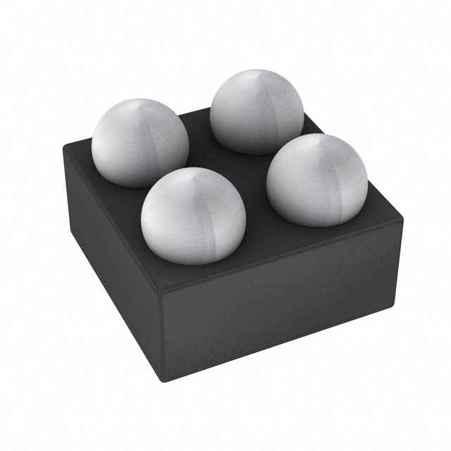
STMicroelectronics LD39030SJ25R

Part No.:
LD39030SJ25R
Manufacturer:
STMicroelectronics
Category:
Voltage Regulators - Linear, Low Drop Out (LDO) Regulators
Package:
4-UFBGA, FCBGA
Datasheet:
AetrixLD39030SJ25R.pdf
Description:
IC REG LIN 2.5V 300MA 4FLIPCHIP
Quantity:
Payment:
Payment
Shipping:
Shipping

Inventory:385

Please send an inquiry. Send us your inquiry, and we will respond immediately.

Part Number
Quantity*
Price
Name*
Company
Email*
Comments

Product details

Overview

LD39030SJ25R from STMicroelectronics is a 300 mA low-noise, low-quiescent-current LDO voltage regulator with fixed 2.5 V output, 200 mV typical dropout at full load, 20 μA typical quiescent current at no load, and 30 μVRMS output noise (1 kHz–100 kHz). It operates from 1.5 V to 5.5 V input, features logic-controlled shutdown, internal soft-start (100 μs), and is stabilized with a 1 μF ceramic output capacitor - ideal for powering RF-sensitive analog rails in portable battery-powered systems.

For engineers reviewing the LD39030SJ25R datasheet, LD39030SJ25R pinout, LD39030SJ25R application, or LD39030SJ25R equivalent, key selection criteria include ultra-low noise performance for ADC/DAC reference supplies, sub-1 μA shutdown current for energy harvesting nodes, dropout behavior under dynamic load, and compatibility with miniature flip-chip packaging in space-constrained handheld designs.

Technical Context

The LD39030SJ25R employs a bandgap-referenced error amplifier with internal trimming (1.22 V reference) and thermal/short-circuit protection. Its flip-chip 4-bump construction enables low-inductance, high-frequency stability with minimal PCB footprint.

It integrates an enable-controlled MOSFET pass device with internal soft-start circuitry that limits inrush current by 67% and ensures monotonic VOUT rise. Supply voltage rejection remains ≥62 dB up to 10 kHz, then rolls off above that frequency due to internal compensation architecture.

Key Specifications

Parameter Value and Actual Design Meaning
Output voltage Fixed 2.5 V ±2.0 % at 25 °C; supports precision analog biasing without external feedback.
Max output current 300 mA guaranteed; sufficient for powering multiple low-power microcontrollers or sensor front-ends.
Dropout voltage 200 mV typ. at 300 mA; enables operation down to VIN = 2.7 V while maintaining regulated 2.5 V output.
Quiescent current 20 μA typ. at no load; extends battery life in always-on wake-up circuits.
Output noise 30 μVRMS (1 kHz–100 kHz); meets stringent noise requirements for high-resolution SAR ADC reference supplies.
Enable threshold VEN high = 0.9 V min.; compatible with 1.2 V, 1.8 V, and 2.5 V logic families without level-shifting.
Operating temperature −40 °C to +125 °C junction; qualified for extended industrial and automotive cabin-adjacent environments.

Pinout & Package

LD39030SJ25R uses a flip-chip 4-bump package (0.8 mm × 0.8 mm, 0.4 mm pitch), with exposed die pad for thermal conduction and minimal parasitic inductance. The package is ECOPACK®-compliant and RoHS-compliant.

Pin/Terminal Circuit Role Design Meaning
A2 (EN) Logic enable input Active-high control: <0.4 V = shutdown (<1 μA IQ), >0.9 V = active; supports direct connection to MCU GPIO.
A1 (GND) Analog/digital ground reference Common return path for input/output currents and internal bandgap reference; requires low-impedance PCB plane connection.
B2 (IN) Regulator input supply Accepts 1.5–5.5 V DC; must be decoupled with ≥1 μF ceramic capacitor close to pin.
B1 (OUT) Regulated output Delivers stable 2.5 V ±2 %; requires 1 μF ceramic capacitor (ESR <2 Ω @ 100 kHz) for stability per Figure 21.

Key Features

Feature Design Value
Ultra-low noise regulation 30 μVRMS output noise enables clean power for 16-bit+ ADCs and RF synthesizer VCO supplies.
Internal soft-start 100 μs controlled ramp eliminates inrush current spikes, preventing brownout on shared battery rails.
Ceramic-capacitor compatibility Stable with 1 μF X5R/X7R ceramic output capacitor - reduces BOM count and board area vs. tantalum solutions.
Sub-μA shutdown mode 0.001–1 μA max. IQ in OFF mode enables multi-year operation in coin-cell–powered IoT endpoints.
Thermal & short-circuit protection Auto-recovery shutdown at 160 °C junction temp and constant-current limiting (~400 mA) prevent catastrophic failure.

Applications

Mobile Phone Baseband Power Digital Still Camera Sensor Bias

Use Scenario: Powering CMOS image sensor analog front-end and PLL reference voltage in compact camera modules.

IC Role / Device Role / Timing Role: Low-noise LDO supplying 2.5 V bias to pixel array and timing generator circuits.

Use Value: 30 μVRMS noise prevents fixed-pattern noise and quantization artifacts in raw image data.

Use Scenario: Providing stable 2.5 V reference for high-speed ADCs digitizing CCD/CMOS sensor outputs.

IC Role / Device Role / Timing Role: Precision voltage source for ADC reference rail, isolated from digital switching noise.

Use Value: ±2.0 % output tolerance and 62 dB PSRR at 1 kHz ensure <0.5 LSB error in 14-bit conversions.

Wearable Health Monitor Analog Front-End Bluetooth LE Audio Codec Power

Use Scenario: Supplying ECG/PPG signal conditioning amplifiers and instrumentation op-amps in ultra-low-power wearables.

IC Role / Device Role / Timing Role: Ultra-low-IQ LDO delivering clean 2.5 V to analog signal chain during continuous sensing.

Use Value: 20 μA no-load IQ extends single-CR2032 battery life beyond 6 months in always-on monitoring mode.

Use Scenario: Powering audio DAC and headphone driver ICs in Bluetooth earbuds with strict EMI constraints.

IC Role / Device Role / Timing Role: Low-EMI, low-noise post-regulator for audio codec VDDIO and AVDD domains.

Use Value: Flip-chip package minimizes radiated emissions; 200 mV dropout preserves headroom for 3.0 V battery discharge curve.

Equivalent & Alternatives

The following parts are listed as comparable options for similar low-noise LDO applications.

Alternative Part Technical Difference Application Difference Selection Advice
Torex XC6210B252MR-G 250 mA max output; 150 mV dropout at 200 mA; 40 μVRMS noise; SOT-25 package (larger footprint). Lacks integrated soft-start; requires external EN pull-up; not qualified for >105 °C ambient. Choose for cost-sensitive, non-automotive consumer devices where 50 mA lower current and higher noise are acceptable.
Analog Devices ADP125ARHZ-2.5-R7 500 mA output; 135 mV dropout at 500 mA; 45 μVRMS noise; 10-pin LFCSP package. Higher quiescent current (35 μA typ. no load); no flip-chip construction; larger thermal resistance (RthJA = 210 °C/W). Prefer when higher output current and wider input range (2.3–5.5 V) outweigh noise and size trade-offs.

Compared with XC6210B252MR-G and ADP125ARHZ-2.5-R7, the LD39030SJ25R uniquely combines 300 mA capability, 30 μVRMS noise, 20 μA IQ, and 0.8 mm × 0.8 mm flip-chip packaging - making it optimal for miniaturized, battery-constrained systems demanding both ultra-low noise and ultra-low power.

Availability

LD39030SJ25R is available at Aetrix Electronics and suitable for mobile phone baseband power, wearable health monitor analog front-ends, digital still camera sensor bias, and Bluetooth LE audio codec power requiring stable component supply across production volumes.

Supply support for LD39030SJ25R includes scheduled delivery planning, volume procurement assistance, BOM continuity management, traceable sourcing, and lifecycle availability coordination for OEM customers, industrial embedded developers, connected-device designers, and electronics production programs.

Manufacturer

STMicroelectronics is a global semiconductor leader headquartered in Geneva, Switzerland, designing and manufacturing silicon solutions for automotive, industrial, and consumer markets since 1987.

The LD390xx series targets ultra-low-power, noise-sensitive portable electronics - emphasizing miniature packaging, sub-μA shutdown, and ceramic-capacitor stability for next-generation battery-operated devices.

FAQ

What is the minimum input voltage required to maintain regulation at 2.5 V output?

The LD39030SJ25R maintains regulation down to VIN = VOUT + VDROP = 2.5 V + 0.2 V = 2.7 V under 300 mA load (typical). At lighter loads, dropout decreases - e.g., ~50 mV at 10 mA - enabling operation from as low as 2.55 V input while sustaining 2.5 V output. Below 1.5 V input, the device shuts down per absolute maximum rating.

Can the LD39030SJ25R be used with a 0.47 μF output capacitor?

No. The datasheet specifies 1 μF minimum ceramic output capacitance (X5R/X7R) for stability, validated in Figure 21's ESR/COUT stability zone. Using 0.47 μF risks oscillation or poor transient response, especially under load steps. A 1 μF capacitor is mandatory; 2.2 μF is acceptable and improves PSRR above 10 kHz.

Does the EN pin require an external pull-up resistor?

No. The EN pin has an internal pull-down (IEN ≤ 100 nA), so it defaults to shutdown when left floating. To activate the regulator, drive EN to ≥0.9 V using a GPIO or dedicated enable signal - no external pull-up is needed or recommended, as it would increase system IQ.

How does thermal shutdown behave during sustained overload?

When junction temperature reaches 160 °C, the device enters thermal shutdown, disabling the pass transistor and reducing output current to near zero. After cooling by ≥20 °C hysteresis, it automatically resumes regulation without requiring an EN toggle. This cycle repeats if overload persists, protecting against permanent damage during solder reflow or sustained short-circuit conditions.

LD39030SJ25R Specifications

Product attributes
Attribute value
Manufacturer:
STMicroelectronics
Series:
-
Package/Case:
4-UFBGA, FCBGA
Packaging:
Tape & Reel (TR)
Product Status:
Obsolete
Output Configuration:
Positive
Output Type:
Fixed
Number of Regulators:
1
Voltage - Input (Max):
5.5V
Voltage - Output (Min/Fixed):
2.5V
Voltage - Output (Max):
-
Voltage Dropout (Max):
0.3V @ 300mA
Current - Output:
300mA
Current - Quiescent (Iq):
50 µA
Current - Supply (Max):
85 µA
PSRR:
62dB (1kHz ~ 10kHz)
Control Features:
Enable
Protection Features:
Over Current, Over Temperature, Soft Start
Operating Temperature:
-40°C ~ 125°C
Grade:
-
Qualification:
-
Mounting Type:
Surface Mount
Supplier Device Package:
4-Flipchip (0.79x0.79)

LD39030SJ25R FAQ

1.How can I place an order for LD39030SJ25R through Aetrix?

Please submit a Request for Quotation (RFQ) for LD39030SJ25R on Aetrix. Our sales agent will provide a competitive quotation and guide you through the order confirmation once you accept the terms.

2.Are the price and stock information for LD39030SJ25R reliable?

The price and inventory of LD39030SJ25R are updated periodically and may fluctuate due to market conditions. Stock and pricing data are typically refreshed every 24 hours. Quotation validity for LD39030SJ25R is usually 5 days.

3.What payment methods are accepted for LD39030SJ25R?

We accept Wire Transfer, PayPal, Credit Card, Western Union, MoneyGram, and Escrow for LD39030SJ25R transactions.

Note: Certain payment methods may incur a processing fee.

4.How is shipping managed for LD39030SJ25R?

LD39030SJ25R orders can be shipped via leading logistics carriers, including DHL, UPS, FedEx, TNT, or Registered Mail.

Once your LD39030SJ25R order is processed, you will receive an email with the shipment details and tracking number.

Note: Tracking information may take up to 24 hours to appear. Express delivery typically takes 3–5 business days.

5.How can I obtain technical support or documentation for LD39030SJ25R?

For technical support, including LD39030SJ25R datasheets, pinout diagrams, or application guidance, please contact our engineering support team. They can provide detailed documentation and assistance for your LD39030SJ25R requirements.

6.How does Aetrix verify that LD39030SJ25R is sourced from the original manufacturer or authorized distributors?

All LD39030SJ25R products on Aetrix are procured from qualified distributors and authorized channels. Our dedicated quality assurance team conducts strict verification, including traceability checks and, if necessary, third-party testing. This ensures that LD39030SJ25R meets industry standards.

7.What is the process for return or replacement of LD39030SJ25R?

All LD39030SJ25R units undergo pre-shipment inspection (PSI). If there is an issue with LD39030SJ25R, returns or replacements are accepted under the following conditions:

1.Quantity discrepancies, incorrect items, or visible external defects (such as breakage or corrosion), acknowledged by Aetrix.

2.The issue is reported within 90 days of delivery.

3.The LD39030SJ25R part is unused and in its original packaging.

Return procedure for LD39030SJ25R:

1.Submit a request within 90 days.

2.Obtain a Return Material Authorization (RMA) from Aetrix.

LD39030SJ25R Tags

  • LD39030SJ25R
  • LD39030SJ25R PDF
  • LD39030SJ25R Datasheet
  • LD39030SJ25R Specifications
  • LD39030SJ25R Images
  • STMicroelectronics
  • STMicroelectronics LD39030SJ25R
  • Buy LD39030SJ25R
  • LD39030SJ25R Price
  • LD39030SJ25R Distributor
  • LD39030SJ25R Supplier
  • LD39030SJ25R Wholesale
Related Products
MIC5504-1.8YM5-TR
MIC5504-1.8YM5-TR

Microchip Technology

MIC5504-3.3YM5-TR
MIC5504-3.3YM5-TR

Microchip Technology

MIC5365-3.0YC5-TR
MIC5365-3.0YC5-TR

Microchip Technology

MIC5365-1.8YC5-TR
MIC5365-1.8YC5-TR

Microchip Technology

MIC5365-2.5YC5-TR
MIC5365-2.5YC5-TR

Microchip Technology

MIC5365-3.3YC5-TR
MIC5365-3.3YC5-TR

Microchip Technology

MIC5365-3.3YD5-TR
MIC5365-3.3YD5-TR

Microchip Technology

MIC5317-3.3YM5-TR
MIC5317-3.3YM5-TR

Microchip Technology

TLV1117LV33DCYR
TLV1117LV33DCYR

Texas Instruments

MIC5317-3.3YMT-TZ
MIC5317-3.3YMT-TZ

Microchip Technology

MIC5528-3.3YMT-TR
MIC5528-3.3YMT-TR

Microchip Technology

TLV75801PDRVR
TLV75801PDRVR

Texas Instruments

Tech Hub

Search

Search

PRODUCT

PRODUCT

PHONE

PHONE

USER

USER