Send an Inquiry

To receive a quote for your project, please fill in the following information, and we’ll get back to you promptly.

Name*
Company*
Email Address*
Phone/WhatsApp
Part Number*
Quantity*
Message
Submit Inventory List

Please fill in the following information, and we’ll get back to you promptly.

Name*
Company*
Email Address*
Phone/WhatsApp
Upload My List
Message

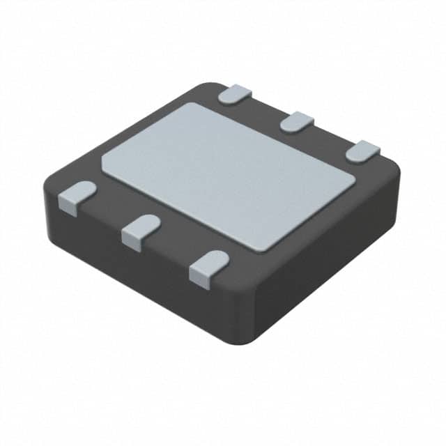
STMicroelectronics LDL112PU18R

Part No.:
LDL112PU18R
Manufacturer:
STMicroelectronics
Category:
Voltage Regulators - Linear, Low Drop Out (LDO) Regulators
Package:
6-WFDFN Exposed Pad
Datasheet:
AetrixLDL112PU18R.pdf
Description:
IC REG LINEAR 1.8V 1.2A 6DFN
Quantity:
Payment:
Payment
Shipping:
Shipping

Inventory:3,388

Please send an inquiry. Send us your inquiry, and we will respond immediately.

Part Number
Quantity*
Price
Name*
Company
Email*
Comments

Product details

Overview

LDL112PU18R from STMicroelectronics is a 1.8 V fixed-output, 1.2 A low-dropout linear regulator with 300 mV typical dropout at 1 A, ±2.0% output voltage accuracy at 25 °C, reverse current protection, and logic-controlled shutdown. It operates from 1.6 V to 5.5 V input and supports ceramic output capacitors as low as 1 µF - ideal for USB-powered portable devices requiring stable low-voltage rail generation.

For engineers reviewing the LDL112PU18R datasheet, LDL112PU18R pinout, LDL112PU18R application, or LDL112PU18R equivalent, key selection considerations include dropout performance at full load, quiescent current in active/off modes (35 µA typ. / <1 µA max.), thermal protection behavior, and compatibility with compact DFN6 (2x2) or PPAK packages in space-constrained battery-powered designs.

Technical Context

The LDL112PU18R uses a PMOS pass transistor architecture enabling true reverse current blocking across all operating states - including shutdown - by actively switching gate and bulk to VOUT when reverse bias occurs. Its internal bandgap reference (800 mV) feeds an error amplifier controlling the pass element, delivering tight line/load regulation (≤0.1 %/V and ≤30 mV) over -40 °C to 125 °C.

Thermal shutdown activates at 165 °C with 20 °C hysteresis, and current limiting clamps short-circuit output to 1.4–2 A. The enable pin (EN) accepts logic-level inputs (VIL ≤ 0.35 V, VIH ≥ 1.4 V), and the exposed pad must be connected to GND for thermal and electrical integrity.

Key Specifications

ParameterValue and Actual Design Meaning
Output VoltageFixed 1.8 V ±2.0% at 25 °C - ensures stable power for 1.8 V logic rails without external feedback components.
Max Output Current1.2 A guaranteed - supports high-current microcontrollers or RF modules in portable systems.
Dropout Voltage300 mV typ. at 1 A - enables operation from single-cell Li-ion (3.0 V min.) or USB 3.3 V supplies with minimal headroom loss.
Quiescent Current35 µA typ. at no-load - extends battery life in always-on sensor nodes or standby circuits.
Shutdown Current<1 µA max. - critical for ultra-low-power wake-on-event applications where leakage must be minimized.
Input Voltage Range1.6 V to 5.5 V - accommodates wide-input sources including boosted battery rails and industrial 3.3/5 V buses.
Output Capacitor1 µF ceramic minimum - reduces BOM count and PCB area vs. electrolytic/tantalum alternatives.

Pinout & Package

LDL112PU18R is available in DFN6 (2x2) mm, DFN6 (3x3) mm, SO8-batwing, and PPAK packages. All variants share identical pin functions and require the exposed pad to be soldered to GND for thermal management and electrical stability.

Pin/TerminalCircuit RoleDesign Meaning
VINLDO input supplyAccepts 1.6–5.5 V; must be decoupled with ≥1 µF ceramic capacitor close to pin.
GNDPower and signal groundCommon return path; exposed pad must be connected to this node for thermal conduction and noise immunity.
ENEnable logic inputActive-high control: low = shutdown (<1 µA IQ), high = regulation; must not float.
VOUTRegulated outputDelivers fixed 1.8 V; requires ≥1 µF ceramic capacitor to ground for stability and transient response.
NCNo-connect terminalNot internally bonded; left unconnected per design - no routing or stitching required.

Key Features

FeatureDesign Value
Reverse current protectionPrevents backflow from VOUT to VIN during off-state or fault conditions - eliminates need for external blocking diode.
Low dropout voltage300 mV typical at 1 A enables efficient use of marginal input voltages (e.g., 2.1 V → 1.8 V rail).
Logic-controlled shutdownEN pin reduces total device current to <1 µA - essential for battery runtime optimization in sleep modes.
Thermal & current protectionAuto-recovering 165 °C shutdown and 1.4–2 A current limit prevent damage under overload or poor heatsinking.
Ceramic capacitor compatibleStable with 1 µF COUT - avoids cost, size, and reliability penalties of larger tantalum or aluminum electrolytics.

Applications

USB-C Peripheral PowerWearable Sensor Node

Use Scenario: Powering BLE SoC, flash memory, and analog front-end from USB-C 5 V via buck-boost + LDL112PU18R post-regulation.

IC Role / Device Role / Timing Role: Final-stage LDO providing clean, low-noise 1.8 V for digital core and I/O domains.

Use Value: Reverse current blocking prevents backfeed into upstream DC-DC during USB disconnect; 35 µA IQ minimizes quiescent drain during deep-sleep intervals.

Use Scenario: Compact fitness tracker with coin-cell battery, accelerometer, and OLED display.

IC Role / Device Role / Timing Role: Primary 1.8 V supply for MCU and sensors, enabled only during activity sampling windows.

Use Value: Sub-1 µA shutdown current extends shelf life; DFN6 (2x2) footprint fits within 8 mm × 8 mm board area constraint.

Industrial IoT Edge ControllerLow-Power Camera Module

Use Scenario: DIN-rail mounted gateway using wide-input 9–36 V supply, regulated down to 3.3 V then to 1.8 V for FPGA configuration memory.

IC Role / Device Role / Timing Role: Point-of-load regulator ensuring tight tolerance and low noise for configuration SRAM interface.

Use Value: ±2.0% output accuracy guarantees reliable boot from SPI flash; thermal protection sustains operation in enclosed enclosures up to 70 °C ambient.

Use Scenario: USB-powered security camera with image sensor, ISP, and Wi-Fi SoC sharing a 1.8 V domain.

IC Role / Device Role / Timing Role: Single LDO powering multiple 1.8 V peripherals simultaneously under dynamic load steps.

Use Value: 30 mV load regulation and fast transient response (<10 µs recovery) prevent sensor frame corruption during burst-mode capture.

Equivalent & Alternatives

The following parts are listed as comparable options for similar LDO regulator applications.

Alternative PartTechnical DifferenceApplication DifferenceSelection Advice
Torex XC6210B182MR-G1.8 V fixed, 1 A max, 250 mV dropout at 1 A, 1 µA shutdown current, SOT-25 package only.Lacks reverse current protection and thermal shutdown; limited to lower-current, non-safety-critical roles.Select when minimal footprint (SOT-25) and ultra-low shutdown current outweigh protection requirements.
Richtek RT9013-18GJ51.8 V fixed, 500 mA max, 200 mV dropout at 300 mA, 25 µA IQ, DFN6 (2x2) package.Half the output current rating; no reverse current blocking; lower thermal robustness (no explicit TSD spec).Choose only for sub-500 mA loads where cost sensitivity dominates over safety and margin.

Compared with XC6210B182MR-G and RT9013-18GJ5, LDL112PU18R uniquely combines 1.2 A capability, reverse current blocking, thermal shutdown, and DFN6 (2x2)/PPAK packaging - making it the sole option for robust, high-current 1.8 V point-of-load regulation in battery- or USB-fed edge devices.

Availability

LDL112PU18R is available at Aetrix Electronics and suitable for USB-powered devices, wearable sensor nodes, and industrial IoT edge controllers requiring stable component supply, long-term lifecycle support, and RoHS-compliant packaging.

Supply support for LDL112PU18R includes scheduled delivery planning, volume procurement assistance, BOM continuity management, traceable sourcing, and lifecycle availability coordination for OEM customers, industrial embedded developers, connected-device designers, and electronics production programs.

Manufacturer

STMicroelectronics is a global semiconductor leader headquartered in Geneva, Switzerland, designing and manufacturing silicon solutions for automotive, industrial, and consumer markets since 1987.

The LDL112 series belongs to ST's high-efficiency, low-quiescent-current LDO portfolio - engineered specifically for battery longevity and system-level reliability in portable and always-on embedded applications.

FAQ

What is the minimum input voltage required for stable 1.8 V output at 1.2 A?

The LDL112PU18R requires VIN ≥ VOUT + VDROP to maintain regulation. With 600 mV maximum dropout at 1.2 A and 125 °C, the minimum input is 1.8 V + 0.6 V = 2.4 V. At room temperature, 2.1 V input suffices due to lower typical dropout (300–350 mV).

Does LDL112PU18R require an external resistor divider for 1.8 V output?

No. LDL112PU18R is the fixed 1.8 V version - it contains internal feedback resistors and does not use the ADJ pin. Only the adjustable versions (e.g., LDL112PVR) require external R1/R2 to set VOUT.

Can LDL112PU18R be used with a 10 µF ceramic output capacitor?

Yes. The datasheet specifies COUT = 1–10 µF ceramic for stability. A 10 µF X7R 0603 capacitor improves transient response and PSRR at higher frequencies while remaining within the recommended ESR range (0.01–2 Ω at 100 kHz).

Is the exposed thermal pad electrically connected internally?

Yes - the exposed pad is internally tied to GND. It must be soldered to a dedicated GND plane on the PCB to ensure proper thermal dissipation (RthJC = 15 °C/W for DFN6 2x2) and to maintain low-noise reference integrity.

LDL112PU18R Specifications

Product attributes
Attribute value
Manufacturer:
STMicroelectronics
Series:
-
Package/Case:
6-WFDFN Exposed Pad
Packaging:
Tape & Reel (TR)
Product Status:
Active
Output Configuration:
Positive
Output Type:
Fixed
Number of Regulators:
1
Voltage - Input (Max):
5.5V
Voltage - Output (Min/Fixed):
1.8V
Voltage - Output (Max):
-
Voltage Dropout (Max):
0.6V @ 1.2A
Current - Output:
1.2A
Current - Quiescent (Iq):
70 µA
Current - Supply (Max):
400 µA
PSRR:
57dB (1kHz)
Control Features:
Enable
Protection Features:
Over Current, Over Temperature, Reverse Current
Operating Temperature:
-40°C ~ 125°C (TJ)
Grade:
-
Qualification:
-
Mounting Type:
Surface Mount
Supplier Device Package:
6-DFN (2x2)

LDL112PU18R FAQ

1.How can I place an order for LDL112PU18R through Aetrix?

Please submit a Request for Quotation (RFQ) for LDL112PU18R on Aetrix. Our sales agent will provide a competitive quotation and guide you through the order confirmation once you accept the terms.

2.Are the price and stock information for LDL112PU18R reliable?

The price and inventory of LDL112PU18R are updated periodically and may fluctuate due to market conditions. Stock and pricing data are typically refreshed every 24 hours. Quotation validity for LDL112PU18R is usually 5 days.

3.What payment methods are accepted for LDL112PU18R?

We accept Wire Transfer, PayPal, Credit Card, Western Union, MoneyGram, and Escrow for LDL112PU18R transactions.

Note: Certain payment methods may incur a processing fee.

4.How is shipping managed for LDL112PU18R?

LDL112PU18R orders can be shipped via leading logistics carriers, including DHL, UPS, FedEx, TNT, or Registered Mail.

Once your LDL112PU18R order is processed, you will receive an email with the shipment details and tracking number.

Note: Tracking information may take up to 24 hours to appear. Express delivery typically takes 3–5 business days.

5.How can I obtain technical support or documentation for LDL112PU18R?

For technical support, including LDL112PU18R datasheets, pinout diagrams, or application guidance, please contact our engineering support team. They can provide detailed documentation and assistance for your LDL112PU18R requirements.

6.How does Aetrix verify that LDL112PU18R is sourced from the original manufacturer or authorized distributors?

All LDL112PU18R products on Aetrix are procured from qualified distributors and authorized channels. Our dedicated quality assurance team conducts strict verification, including traceability checks and, if necessary, third-party testing. This ensures that LDL112PU18R meets industry standards.

7.What is the process for return or replacement of LDL112PU18R?

All LDL112PU18R units undergo pre-shipment inspection (PSI). If there is an issue with LDL112PU18R, returns or replacements are accepted under the following conditions:

1.Quantity discrepancies, incorrect items, or visible external defects (such as breakage or corrosion), acknowledged by Aetrix.

2.The issue is reported within 90 days of delivery.

3.The LDL112PU18R part is unused and in its original packaging.

Return procedure for LDL112PU18R:

1.Submit a request within 90 days.

2.Obtain a Return Material Authorization (RMA) from Aetrix.

LDL112PU18R Tags

  • LDL112PU18R
  • LDL112PU18R PDF
  • LDL112PU18R Datasheet
  • LDL112PU18R Specifications
  • LDL112PU18R Images
  • STMicroelectronics
  • STMicroelectronics LDL112PU18R
  • Buy LDL112PU18R
  • LDL112PU18R Price
  • LDL112PU18R Distributor
  • LDL112PU18R Supplier
  • LDL112PU18R Wholesale
Related Products
MIC5504-1.8YM5-TR
MIC5504-1.8YM5-TR

Microchip Technology

MIC5504-3.3YM5-TR
MIC5504-3.3YM5-TR

Microchip Technology

MIC5365-3.0YC5-TR
MIC5365-3.0YC5-TR

Microchip Technology

MIC5365-1.8YC5-TR
MIC5365-1.8YC5-TR

Microchip Technology

MIC5365-2.5YC5-TR
MIC5365-2.5YC5-TR

Microchip Technology

MIC5365-3.3YC5-TR
MIC5365-3.3YC5-TR

Microchip Technology

MIC5365-3.3YD5-TR
MIC5365-3.3YD5-TR

Microchip Technology

MIC5317-3.3YM5-TR
MIC5317-3.3YM5-TR

Microchip Technology

TLV1117LV33DCYR
TLV1117LV33DCYR

Texas Instruments

MIC5317-3.3YMT-TZ
MIC5317-3.3YMT-TZ

Microchip Technology

MIC5528-3.3YMT-TR
MIC5528-3.3YMT-TR

Microchip Technology

TLV75801PDRVR
TLV75801PDRVR

Texas Instruments

Tech Hub

Search

Search

PRODUCT

PRODUCT

PHONE

PHONE

USER

USER