Send an Inquiry

To receive a quote for your project, please fill in the following information, and we’ll get back to you promptly.

Name*
Company*
Email Address*
Phone/WhatsApp
Part Number*
Quantity*
Message
Submit Inventory List

Please fill in the following information, and we’ll get back to you promptly.

Name*
Company*
Email Address*
Phone/WhatsApp
Upload My List
Message

Qorvo QPB9350TR13

Part No.:
QPB9350TR13
Manufacturer:
Qorvo
Category:
RF Front End (LNA + PA)
Package:
32-VFQFN Exposed Pad
Datasheet:
AetrixQPB9350TR13.pdf
Description:
0.7-1.0 DUAL CHANNEL DVGA
Quantity:
Payment:
Payment
Shipping:
Shipping

Inventory:1,653

Please send an inquiry. Send us your inquiry, and we will respond immediately.

Part Number
Quantity*
Price
Name*
Company
Email*
Comments

Product details

Overview

QPB9350TR13 from Qorvo is a dual-channel receive variable gain amplifier (Rx VGA) system-in-package for macro base station receivers, operating from 0.4–1.0 GHz. It integrates two independent LNA chains-each with first-stage E-pHEMT LNA (0.4 dB NF), digital step attenuator (31 dB range in 1 dB steps), and second-stage LNA-plus dedicated shutdown pins per channel and SPI control. Used in TDD/FDD diversity receiver front-ends requiring high linearity (OIP3 up to +38.5 dBm) and ultra-low noise.

For engineers reviewing the QPB9350TR13 datasheet, pinout, applications, or equivalent options, key selection criteria include dual-channel isolation (40 dB), 5 V supply compatibility, +1.8 V logic-level SPI interface, thermal resistance (15 °C/W), and RoHS-compliant 5×5 mm 32-pin leadless SMT package.

Technical Context

The QPB9350TR13 implements a two-stage cascaded architecture per channel: LNA1 provides ultra-low-noise amplification (0.4 dB NF at 900 MHz), followed by a digitally controlled DSA and LNA2 for gain flexibility and output drive. Each channel features independent power-down via dedicated VPD_M/VPD_D pins, enabling precise TDD timing control with 80 ns switching speed.

SPI-based register control (24-bit, MSB-first, 4-wire optional) configures DSA settings (5-bit main/diversity controls), power modes, and read-back functions. The device supports streaming and single-instruction modes, with internal double-buffered registers updated only on transfer-bit assertion to prevent mid-operation glitches.

Key Specifications

ParameterValue and Actual Design Meaning
Freq. Range0.4–1.0 GHz: Full specified performance across cellular bands including 700 MHz, 800 MHz, 900 MHz, and 1.0 GHz.
LNA1 Noise Figure0.4 dB typ. at 900 MHz: Enables high sensitivity in weak-signal macro base station reception.
OIP3 (LNA2)+38.5 dBm typ. at 900 MHz: Supports high dynamic range in dense RF environments without intermodulation distortion.
Gain Control31 dB range in 1 dB steps: Enables precise AGC implementation with minimal quantization error in closed-loop systems.
Supply Voltage+5.0 V ±0.25 V: Compatible with standard telecom power rails; VDD_SPI must be powered before serial lines.
Thermal Resistance15 °C/W (θjc): Requires thermal vias under backside paddle for reliable operation at 400 mA max current and 105 °C case temperature.
Channel Isolation40 dB min.: Prevents crosstalk between main and diversity paths in MIMO and diversity receiver architectures.

Pinout & Package

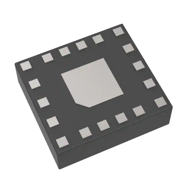
QPB9350TR13 is housed in a RoHS-compliant, 5 mm × 5 mm, 32-pin surface-mount leadless package with exposed backside paddle for RF grounding and thermal dissipation. Recommended PCB layout includes ≥12 thermal vias (0.25 mm plated diameter) under the paddle.

Pin/TerminalCircuit RoleDesign Meaning
RFIN_M / RFIN_DMain/diversity RF inputDC-blocked inputs to first-stage LNAs; require external band-specific matching networks.
LNA1_OUT_M / LNA1_OUT_DLNA1 output & bias nodeDC-biased RF outputs feeding DSA inputs; require external choke + DC block.
DSA_IN_M / DSA_IN_DDSA RF inputInputs to digital step attenuators; DC-blocked, matched for optimal attenuation accuracy.
LNA2_OUT_M / LNA2_OUT_DLNA2 output & bias nodeFinal RF outputs with integrated DC bias; require external choke + DC block for system interface.
VPD_M / VPD_DChannel shutdown controlLogic-level pins (0–0.63 V ON, 1.17–3.0 V OFF) enabling <80 ns LNA enable/disable for TDD timing.
SCLK / CSB / SDIO / SDOSPI interface24-bit MSB-first serial interface; SDO optional (3-/4-wire mode); VIH = 1.2–VDD_SPI, VIL ≤ 0.5 V.
VDD_SPIDedicated SPI supply+5 V rail isolated from main VDD; must power up before SPI signals to avoid reset failure.
GND (Pins 2,9,11–12,14–15,17,19–22,26–27,29–30,32 + paddle)RF/DC groundAll GND pins internally connected; paddle must be soldered with thermal vias to inner ground planes.

Key Features

FeatureDesign Value
Dual independent Rx chainsEnables simultaneous main/diversity signal processing with >40 dB isolation-critical for LTE/NR MIMO and interference rejection.
E-pHEMT LNA1 technologyDelivers 0.4 dB NF at 900 MHz, directly improving receiver sensitivity and SINAD in low-SNR macro cell deployments.
31 dB DSA with 1 dB resolutionSupports fine-grained automatic gain control (AGC) with <±0.5 dB + 5% attenuation error-reducing calibration overhead in production.
Independent VPD control per channelAllows asymmetric power sequencing (e.g., main active while diversity in sleep), reducing average power in TDD burst-mode operation.
Integrated SPI register setDouble-buffered configuration registers (0x10/0x11 for DSA control) prevent gain transients during live updates in deployed systems.

Applications

Macro Base Station ReceiversDiversity Receiver Front-Ends

Use Scenario: High-power outdoor base stations serving multi-sector cells in 4G/5G networks operating across 700–1000 MHz bands.

IC Role / Device Role / Timing Role: Dual-channel Rx VGA providing programmable gain, noise suppression, and TDD-aware shutdown in the first IF stage after antenna diplexers.

Use Value: Enables 0.4 dB NF and +38.5 dBm OIP3 simultaneously-extending coverage radius and supporting higher-order modulation (256-QAM) under interference.

Use Scenario: Dual-antenna receiver configurations using spatial diversity to mitigate multipath fading in urban macro cells.

IC Role / Device Role / Timing Role: Independent main/diversity signal conditioning block with synchronized gain control and isolation >40 dB to preserve correlation independence.

Use Value: Improves link budget by ≥3 dB in fading channels without increasing BOM count-replacing discrete LNA+DSA+LNA solutions with single SiP.

TDD-Based Small CellsFDD Infrastructure Repeaters

Use Scenario: Low-power remote radio units (RRUs) in time-division duplex systems requiring fast LNA enable/disable to match UL/DL slot boundaries.

IC Role / Device Role / Timing Role: TDD timing-critical VGA with 80 ns VPD response and dedicated shutdown pins per channel for precise slot-edge switching.

Use Value: Eliminates need for external gate drivers or discrete shutdown FETs-reducing latency, component count, and PCB area in compact RRUs.

Use Scenario: Bidirectional in-building repeaters amplifying both uplink and downlink simultaneously in frequency-division duplex systems.

IC Role / Device Role / Timing Role: High-isolation dual-channel front-end preventing self-oscillation and intermodulation between UL and DL paths.

Use Value: Achieves >40 dB channel isolation and +36.5 dBm OIP3-enabling stable wideband repeater operation without manual tuning or isolators.

Equivalent & Alternatives

The following parts are listed as comparable options for similar dual-channel Rx VGA applications.

Alternative PartTechnical DifferenceApplication DifferenceSelection Advice
QPB9348TR13Narrower 0.6–1.0 GHz range; identical 32-pin 5×5 mm package and SPI interface; 0.5 dB higher NF (0.9 dB typ.)Optimized for 600–1000 MHz bands only; not suitable for sub-600 MHz 700 MHz low-band deployments.Select QPB9348TR13 only when operating strictly above 600 MHz and lower NF is not required.
SKY77762-31Single-channel 0.4–1.0 GHz VGA; 24-pin 4×4 mm QFN; no integrated DSA; uses analog gain control instead of SPIRequires external DAC and control logic; lacks per-channel shutdown and digital calibration support.Choose SKY77762-31 only for cost-sensitive single-path designs where digital configurability and dual-channel integration are unnecessary.

Compared with QPB9350TR13, QPB9348TR13 trades bandwidth for marginally lower integration, while SKY77762-31 sacrifices channel count, digital control, and noise performance for footprint reduction-making QPB9350TR13 the only option supporting full 0.4–1.0 GHz dual-channel operation with SPI-configurable 31 dB gain control and 0.4 dB NF.

Availability

QPB9350TR13 is available at Aetrix Electronics and suitable for macro base station receivers, diversity front-ends, and TDD/FDD infrastructure requiring stable component supply, long-lifecycle assurance, and RoHS-compliant 5×5 mm packaging.

Supply support for QPB9350TR13 includes scheduled delivery planning, volume procurement assistance, BOM continuity management, traceable sourcing, and lifecycle availability coordination for OEM customers, industrial embedded developers, connected-device designers, and electronics production programs.

Manufacturer

Qorvo is a U.S.-based semiconductor company specializing in RF solutions for wireless infrastructure, defense, and mobile devices, with leadership in GaAs, GaN, and SOI process technologies.

The QPB9350TR13 belongs to Qorvo's macro base station front-end module product line, designed specifically to replace multi-component discrete receiver chains with integrated, thermally robust, digitally controllable SiPs for 4G/5G deployment.

FAQ

What is the absolute maximum RF input power rating for QPB9350TR13?

The absolute maximum CW RF input power for QPB9350TR13 is +20 dBm into 50 Ω at 25 °C. Exceeding this level risks permanent damage to the E-pHEMT LNAs. For continuous operation, design to stay within the recommended input P1dB range (e.g., +22.9 dBm for LNA1 at 700 MHz) and apply external limiting if transient overloads are expected. Always verify matching network insertion loss and reflection coefficients to ensure actual device input power remains within spec.

Does QPB9350TR13 support 3-wire or 4-wire SPI mode?

Yes, QPB9350TR13 supports both 3-wire and 4-wire SPI modes. The SDO pin is optional and enabled via register 0x00 bit [4] (SDO Active). When disabled (default), the device operates in 3-wire mode using SDIO for bidirectional data. When enabled, it uses separate SDIO (input) and SDO (output) lines for full-duplex operation. Clock polarity and phase are fixed (CPOL=0, CPHA=0), and all transfers are 24-bit MSB-first with minimum SCLK period of 50 ns.

How is thermal management implemented in QPB9350TR13?

QPB9350TR13 uses an exposed backside paddle as its primary thermal path, with a junction-to-case thermal resistance (θjc) of 15 °C/W. Reliable thermal performance requires soldering the paddle to a solid ground plane using ≥12 thermal vias (0.25 mm finished diameter) placed in the recommended footprint pattern. PCB layout must use ≥1 oz copper on top and bottom layers, and the device must operate within TCASE = –40 to +105 °C. Derating applies above 85 °C ambient.

Can QPB9350TR13 be used in 700 MHz low-band 5G deployments?

Yes, QPB9350TR13 is fully specified and characterized from 400–1000 MHz, including 700 MHz low-band 5G (n12/n13/n14/n28/n71). At 700 MHz, typical performance includes 24.8 dB gain (LNA1), 0.44 dB NF, +36.2 dBm OIP3, and 24.6 dB input return loss on the QPB9350EVB evaluation board. Band-specific external matching is required on RFIN_M/RFIN_D to optimize noise and return loss-reference design files are available from Qorvo.

What is the function of pins 18 (VPD_D) and 23 (VPD_M) on QPB9350TR13?

Pins 18 (VPD_D) and 23 (VPD_M) are dedicated voltage-controlled shutdown inputs for the diversity and main channel LNAs respectively. Applying 0–0.63 V enables the LNA chain; applying 1.17–3.0 V disables it. Switching occurs in ≤80 ns, making QPB9350TR13 suitable for TDD systems. These pins are independent-allowing asymmetric operation (e.g., main active while diversity off) without affecting the other channel's gain or bias state.

QPB9350TR13 Specifications

Product attributes
Attribute value
Manufacturer:
Qorvo
Series:
-
Packaging:
Tape & Reel (TR)
Product Status:
Active
RF Type:
General Purpose
Frequency:
400MHz ~ 1GHz
Features:
-
Grade:
-
Qualification:
-
Supplier Device Package:
32-SMT (5x5)

QPB9350TR13 FAQ

1.How can I place an order for QPB9350TR13 through Aetrix?

Please submit a Request for Quotation (RFQ) for QPB9350TR13 on Aetrix. Our sales agent will provide a competitive quotation and guide you through the order confirmation once you accept the terms.

2.Are the price and stock information for QPB9350TR13 reliable?

The price and inventory of QPB9350TR13 are updated periodically and may fluctuate due to market conditions. Stock and pricing data are typically refreshed every 24 hours. Quotation validity for QPB9350TR13 is usually 5 days.

3.What payment methods are accepted for QPB9350TR13?

We accept Wire Transfer, PayPal, Credit Card, Western Union, MoneyGram, and Escrow for QPB9350TR13 transactions.

Note: Certain payment methods may incur a processing fee.

4.How is shipping managed for QPB9350TR13?

QPB9350TR13 orders can be shipped via leading logistics carriers, including DHL, UPS, FedEx, TNT, or Registered Mail.

Once your QPB9350TR13 order is processed, you will receive an email with the shipment details and tracking number.

Note: Tracking information may take up to 24 hours to appear. Express delivery typically takes 3–5 business days.

5.How can I obtain technical support or documentation for QPB9350TR13?

For technical support, including QPB9350TR13 datasheets, pinout diagrams, or application guidance, please contact our engineering support team. They can provide detailed documentation and assistance for your QPB9350TR13 requirements.

6.How does Aetrix verify that QPB9350TR13 is sourced from the original manufacturer or authorized distributors?

All QPB9350TR13 products on Aetrix are procured from qualified distributors and authorized channels. Our dedicated quality assurance team conducts strict verification, including traceability checks and, if necessary, third-party testing. This ensures that QPB9350TR13 meets industry standards.

7.What is the process for return or replacement of QPB9350TR13?

All QPB9350TR13 units undergo pre-shipment inspection (PSI). If there is an issue with QPB9350TR13, returns or replacements are accepted under the following conditions:

1.Quantity discrepancies, incorrect items, or visible external defects (such as breakage or corrosion), acknowledged by Aetrix.

2.The issue is reported within 90 days of delivery.

3.The QPB9350TR13 part is unused and in its original packaging.

Return procedure for QPB9350TR13:

1.Submit a request within 90 days.

2.Obtain a Return Material Authorization (RMA) from Aetrix.

QPB9350TR13 Tags
  • QPB9350TR13
  • QPB9350TR13 PDF
  • QPB9350TR13 Datasheet
  • QPB9350TR13 Specifications
  • QPB9350TR13 Images
  • Qorvo
  • Qorvo QPB9350TR13
  • Buy QPB9350TR13
  • QPB9350TR13 Price
  • QPB9350TR13 Distributor
  • QPB9350TR13 Supplier
  • QPB9350TR13 Wholesale
Related Products
RFX2401C
RFX2401C

Skyworks Solutions Inc.

NRF21540-QDAA-R
NRF21540-QDAA-R

Nordic Semiconductor ASA

NRF21540-QDAA-R7
NRF21540-QDAA-R7

Nordic Semiconductor ASA
RFX2411N
RFX2411N

Skyworks Solutions Inc.

SE2438T-R
SE2438T-R

Skyworks Solutions Inc.

SKY66118-11
SKY66118-11

Skyworks Solutions Inc.

SKY85712-21
SKY85712-21

Skyworks Solutions Inc.

SKY85329-11
SKY85329-11

Skyworks Solutions Inc.

SKY66422-11
SKY66422-11

Skyworks Solutions Inc.

SKY66119-11
SKY66119-11

Skyworks Solutions Inc.

NJG1156PCD-TE1
NJG1156PCD-TE1

Nisshinbo Micro Devices Inc.
SE2435L-R
SE2435L-R

Skyworks Solutions Inc.

Tech Hub

Search

Search

PRODUCT

PRODUCT

PHONE

PHONE

USER

USER