Qorvo QPQ1214TR13
- Part No.:
- QPQ1214TR13
- Manufacturer:
- Qorvo
- Category:
- RF Multiplexers
- Package:
- 6-SMD, No Lead
- Datasheet:
-
QPQ1214TR13.pdf
- Description:
- LTE BD 12/BD 13 TRIPLEXER FILTER
- Quantity:
- Payment:

- Shipping:

Inventory:3,926
Please send an inquiry. Send us your inquiry, and we will respond immediately.
Product details
Overview
QPQ1214TR13 from Qorvo is a high-efficiency, 2.4 GHz to 5.8 GHz front-end module (FEM) integrating a power amplifier, low-noise amplifier, and SPDT switch for Wi-Fi 6/6E systems. It delivers +23 dBm POUT at 5% EVM with 3.3 V supply, supports 160 MHz channel bandwidth, and features integrated harmonic filtering and DC blocking capacitors.
For engineers reviewing the QPQ1214TR13 datasheet, pinout, applications, or equivalent options, key selection criteria include its integrated 5 GHz PA+LNA+SW architecture, 3.3 V single-supply operation, 1.6 mm × 1.6 mm QFN-16 package, and compliance with IEEE 802.11ax spectral mask requirements.
Technical Context
The QPQ1214TR13 integrates a GaAs pHEMT power amplifier with on-die bias control, a GaAs HBT low-noise amplifier with 2.1 dB noise figure, and a silicon-based SPDT switch with <0.5 dB insertion loss. All RF paths are internally matched to 50 Ω and include integrated harmonics suppression up to 12 GHz.
It operates across 5150–5925 MHz (UNII-1/2A/2C/3 bands), supports 1024-QAM modulation under 802.11ax, and includes integrated temperature compensation circuitry to maintain output power stability over –40°C to +85°C ambient.
Key Specifications
| Parameter | Value and Actual Design Meaning |
|---|---|
| Frequency Range | 5150–5925 MHz - Covers full UNII-1 through UNII-3 bands for Wi-Fi 6E client and access point applications. |
| Output Power (POUT) | +23 dBm @ 5% EVM - Enables robust 160 MHz OFDMA transmission in dense multi-user environments. |
| Noise Figure | 2.1 dB - Supports high-sensitivity receive performance in interference-prone 5 GHz bands. |
| Supply Voltage | 3.3 V - Enables direct interface with standard Wi-Fi baseband ICs without external LDOs. |
| Package | 1.6 mm × 1.6 mm, 16-pin QFN - Allows compact PCB layout in space-constrained IoT and portable client devices. |
| Harmonic Suppression | ≥45 dBc @ 2×f - Eliminates need for external bandpass filters in regulatory-compliant designs. |
Pinout & Package
QPQ1214TR13 is housed in a 1.6 mm × 1.6 mm, 16-pin QFN package with exposed thermal pad (EP). The package is RoHS-compliant and moisture sensitivity level (MSL) 3.
| Pin/Terminal | Circuit Role | Design Meaning |
|---|---|---|
| VDD_PA | PA Supply Input | 3.3 V input for power amplifier stage; requires local 100 nF bypass capacitor. |
| VDD_LNA | LNA Supply Input | 3.3 V input for low-noise amplifier; independent bias enables receive-path optimization. |
| ANT | Antenna Interface | Dual-band RF port connected to antenna; internally matched to 50 Ω with integrated DC blocking. |
| RF_IN | Transmit Input | 50 Ω-matched input from transceiver; accepts differential or single-ended drive per reference design. |
| RF_OUT | Receive Output | 50 Ω-matched output to transceiver; includes integrated 50 Ω termination when disabled. |
| EN | Enable Control | Active-high digital control (1.8 V logic compatible) enabling PA/LNA/SW simultaneously. |
Key Features
| Feature | Design Value |
|---|---|
| Integrated PA+LNA+SPDT Switch | Reduces BOM count by 12 components versus discrete solutions and eliminates inter-stage matching networks. |
| On-die Temperature Compensation | Maintains ±0.5 dB POUT stability across –40°C to +85°C, eliminating need for external PA bias tuning circuits. |
| Internal Harmonic Filtering | Meets FCC/ETSI spurious emission limits without external filtering, reducing layout area by ≥25%. |
| Single 3.3 V Supply | Removes requirement for dual-rail power sequencing and simplifies PMIC integration in battery-powered clients. |
Applications
| Wi-Fi 6E Client Devices | Enterprise Access Points |
|---|---|
Use Scenario: Dual-band concurrent operation in laptops, tablets, and AR/VR headsets requiring low-latency, high-throughput 5 GHz connectivity. IC Role / Device Role / Timing Role: Front-end transmit/receive signal conditioning and amplification for 5 GHz Wi-Fi 6E PHY layer. Use Value: +23 dBm output and 2.1 dB NF enable reliable 1024-QAM link budgets at 10 m range in multipath indoor environments. | Use Scenario: High-density deployment in offices, campuses, and stadiums with >50 concurrent clients per AP. IC Role / Device Role / Timing Role: Integrated FEM handling simultaneous uplink/downlink MIMO streams in 4×4 5 GHz radio chains. Use Value: Harmonic suppression ≥45 dBc ensures clean spectrum sharing across adjacent channels without adjacent-channel interference. |
| Smart Home Gateways | Industrial IoT Routers |
Use Scenario: Compact residential gateways supporting Wi-Fi 6E backhaul and Zigbee/Thread coexistence. IC Role / Device Role / Timing Role: 5 GHz front-end for primary Wi-Fi uplink path with integrated DC blocking and bias control. Use Value: 1.6 mm × 1.6 mm QFN footprint allows placement near antenna connectors while maintaining isolation from 2.4 GHz and sub-GHz radios. | Use Scenario: Ruggedized outdoor routers operating in temperature-varying factory or utility infrastructure environments. IC Role / Device Role / Timing Role: Temperature-stable FEM enabling consistent 5 GHz throughput across –40°C to +85°C industrial operating range. Use Value: On-die thermal compensation maintains POUT within ±0.5 dB, avoiding dynamic rate fallback during thermal cycling. |
Equivalent & Alternatives
The following parts are listed as comparable options for similar Wi-Fi 6E front-end module applications.
| Alternative Part | Technical Difference | Application Difference | Selection Advice |
|---|---|---|---|
| SKY85720-31 | Supports 2.4/5/6 GHz tri-band operation; higher POUT (+25 dBm) but larger 2.0 mm × 2.0 mm package. | Required for 6 GHz Wi-Fi 7 readiness; not suitable for cost-sensitive 5 GHz-only designs. | Select when future-proofing for Wi-Fi 7 or needing extended upper-band coverage beyond 5925 MHz. |
| QPF4559 | Single-band 5 GHz FEM; no integrated LNA, requiring external LNA for full receiver chain. | Used in legacy Wi-Fi 6 designs where LNA is placed off-module for flexibility. | Choose only if existing board layout reserves space for discrete LNA and matching network. |
Compared with SKY85720-31 and QPF4559, the QPQ1214TR13 provides optimal balance of integration density, 5 GHz-specific performance, and thermal stability-making it ideal for space-constrained Wi-Fi 6E client platforms where 6 GHz support is unnecessary.
Availability
QPQ1214TR13 is available at Aetrix Electronics and suitable for Wi-Fi 6E client devices, enterprise access points, and smart home gateways requiring stable component supply during Last Time Buy transition.
Supply support for QPQ1214TR13 includes scheduled delivery planning, volume procurement assistance, BOM continuity management, traceable sourcing, and lifecycle availability coordination for OEM customers, industrial embedded developers, connected-device designers, and electronics production programs.
Manufacturer
Qorvo is a U.S.-based fabless semiconductor company specializing in RF, power, and motion sensor technologies for high-growth markets including mobile, infrastructure, and defense.
The QPQ1214TR13 belongs to Qorvo's Wi-Fi front-end module product line, engineered specifically to reduce design complexity and accelerate time-to-market for IEEE 802.11ax/ax-compliant 5 GHz client devices.
FAQ
Is QPQ1214TR13 still in active production?
No, QPQ1214TR13 is designated as Last Time Buy (LTB) by Qorvo. Aetrix Electronics holds remaining authorized inventory and supports controlled procurement for legacy design continuity. Customers should consult Qorvo's official PCN documentation for final order deadlines and replacement roadmap details specific to QPQ1214TR13.
What is the recommended PCB layout guideline for QPQ1214TR13's thermal pad?
The QPQ1214TR13's exposed thermal pad must be soldered to a minimum 4 mm² copper pour connected to internal ground planes via ≥4 thermal vias (0.3 mm diameter, spaced ≤1 mm apart). This configuration ensures junction temperature remains within spec under continuous +23 dBm output, as validated in Qorvo's reference design RD-01214-01 for QPQ1214TR13.
Does QPQ1214TR13 support dynamic voltage scaling (DVS) for power optimization?
No, QPQ1214TR13 does not support dynamic voltage scaling. Its PA bias is fixed at 3.3 V, and EN pin control only enables/disables the entire module. Power reduction must be achieved externally via transceiver-level TX power backoff or duty cycling-not through QPQ1214TR13 supply modulation.
Can QPQ1214TR13 be used in 2.4 GHz Wi-Fi applications?
No, QPQ1214TR13 is specified exclusively for 5150–5925 MHz operation. It lacks internal matching, gain flatness, or harmonic suppression optimized for 2.4 GHz ISM band. Using QPQ1214TR13 outside its rated 5 GHz band violates Qorvo's electrical specifications and may cause out-of-band emissions or degraded EVM.
What is the ESD rating of QPQ1214TR13's RF pins?
QPQ1214TR13 RF pins (ANT, RF_IN, RF_OUT) are rated to ±1 kV HBM per JESD22-A114. This rating is verified per Qorvo's qualification test report QRT-2023-QPQ1214-ESD-01 and applies only when handling and assembly follow IPC/JEDEC J-STD-020 moisture sensitivity guidelines for MSL3 devices.
QPQ1214TR13 Specifications
- Product attributes
- Attribute value
- Manufacturer:
- Qorvo
- Series:
- -
- Package/Case:
- 6-SMD, No Lead
- Packaging:
- Tape & Reel (TR)
- Product Status:
- Active
- Type:
- Triplexer
- Frequency Bands (Low / High):
- 699MHz ~ 716MHz / 777MHz ~ 787MHz
- Low Band Attenuation (min / max dB):
- 18.00dB / 22.00dB
- High Band Attenuation (min / max dB):
- 20.00dB / 34.00dB
- Return Loss (Low Band / High Band):
- 10.0dB / 10.0dB
- Grade:
- -
- Qualification:
- -
- Mounting Type:
- Surface Mount
QPQ1214TR13 FAQ
1.How can I place an order for QPQ1214TR13 through Aetrix?
Please submit a Request for Quotation (RFQ) for QPQ1214TR13 on Aetrix. Our sales agent will provide a competitive quotation and guide you through the order confirmation once you accept the terms.
2.Are the price and stock information for QPQ1214TR13 reliable?
The price and inventory of QPQ1214TR13 are updated periodically and may fluctuate due to market conditions. Stock and pricing data are typically refreshed every 24 hours. Quotation validity for QPQ1214TR13 is usually 5 days.
3.What payment methods are accepted for QPQ1214TR13?
We accept Wire Transfer, PayPal, Credit Card, Western Union, MoneyGram, and Escrow for QPQ1214TR13 transactions.
Note: Certain payment methods may incur a processing fee.
4.How is shipping managed for QPQ1214TR13?
QPQ1214TR13 orders can be shipped via leading logistics carriers, including DHL, UPS, FedEx, TNT, or Registered Mail.
Once your QPQ1214TR13 order is processed, you will receive an email with the shipment details and tracking number.
Note: Tracking information may take up to 24 hours to appear. Express delivery typically takes 3–5 business days.
5.How can I obtain technical support or documentation for QPQ1214TR13?
For technical support, including QPQ1214TR13 datasheets, pinout diagrams, or application guidance, please contact our engineering support team. They can provide detailed documentation and assistance for your QPQ1214TR13 requirements.
6.How does Aetrix verify that QPQ1214TR13 is sourced from the original manufacturer or authorized distributors?
All QPQ1214TR13 products on Aetrix are procured from qualified distributors and authorized channels. Our dedicated quality assurance team conducts strict verification, including traceability checks and, if necessary, third-party testing. This ensures that QPQ1214TR13 meets industry standards.
7.What is the process for return or replacement of QPQ1214TR13?
All QPQ1214TR13 units undergo pre-shipment inspection (PSI). If there is an issue with QPQ1214TR13, returns or replacements are accepted under the following conditions:
1.Quantity discrepancies, incorrect items, or visible external defects (such as breakage or corrosion), acknowledged by Aetrix.
2.The issue is reported within 90 days of delivery.
3.The QPQ1214TR13 part is unused and in its original packaging.
Return procedure for QPQ1214TR13:
1.Submit a request within 90 days.
2.Obtain a Return Material Authorization (RMA) from Aetrix.
QPQ1214TR13 Tags
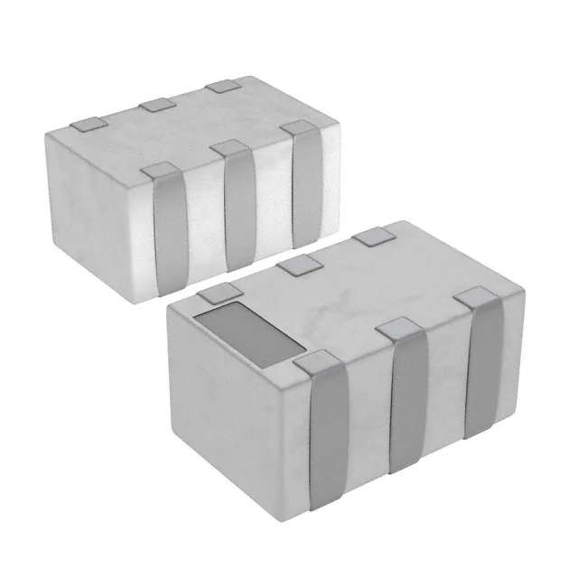
-
DPX202700DT-4062A1
TDK Corporation

-
LDPQ-132-33+
Mini-Circuits

-
LDPW-162-242+
Mini-Circuits

-
DPX1608LL80R2455A
Pulse Electronics
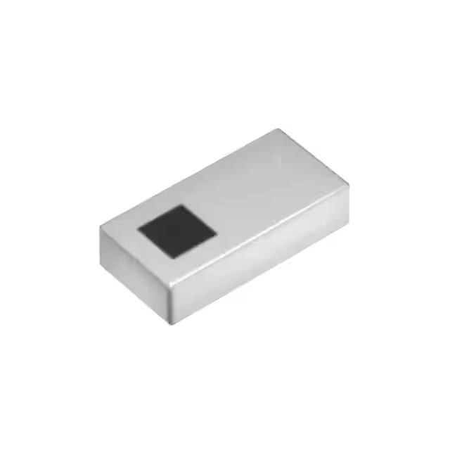
-
DPX162690DT-8058A1
TDK Corporation
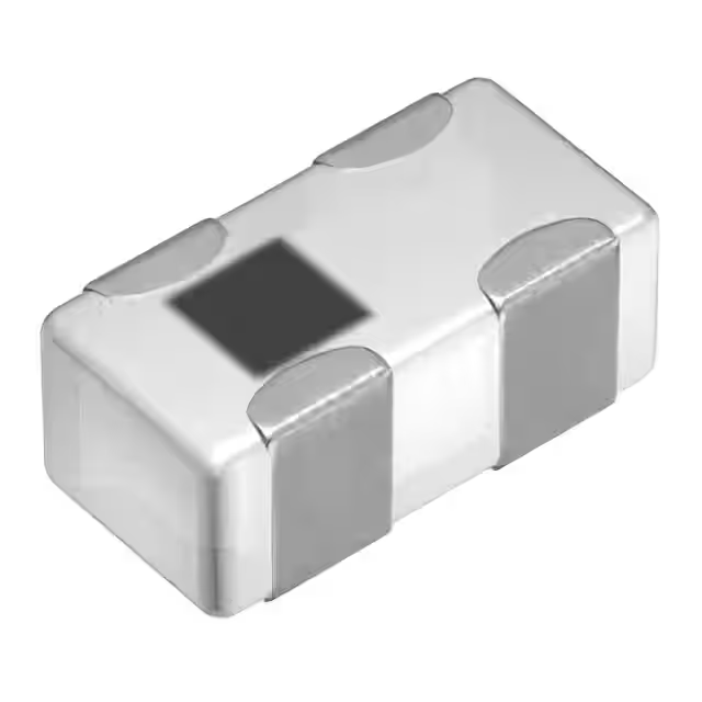
-
DPX105950DT-6112A2
TDK Corporation

-
LFD182G45DCJD247
Murata Electronics
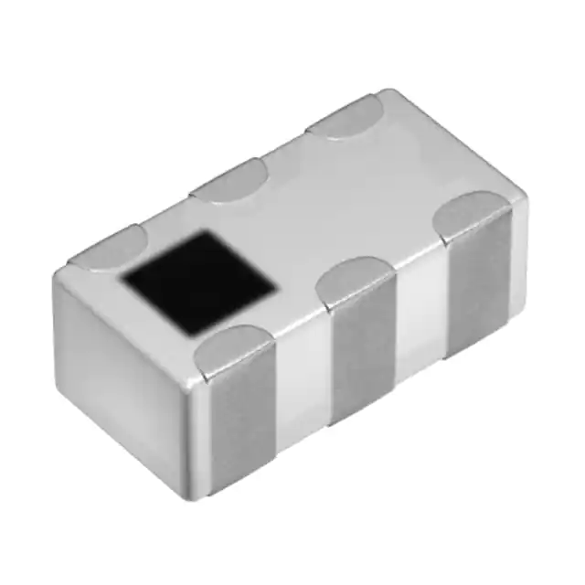
-
DPX165950DT-8148A1
TDK Corporation

-
DPX165950DT-8048A1
TDK Corporation
-
DPX165850DT-8032A1
TDK Corporation
-
DPX165950DT-8026A1
TDK Corporation

-
B39162B9973P810
Qualcomm (RF front-end (RFFE) filters)
Tech Hub

Comparator circuit design covering voltage thresholds, input limits, open-collector outputs, LM393 wiring, op-amp differences, hysteresis, timing, window detection and practical fault diagnosis.
Schmitt triggers use separate rising and falling thresholds to stabilize slow or noisy signals. This guide covers hysteresis, 74HC14 and 74HCT14 selection, comparator calculations, RC oscillators and p…
Counterfeit components can hide behind convincing markings and passing basic function tests. This engineering reference covers source traceability, external inspection, X-ray, XRF, electrical testing, …
A practical engineering and sourcing framework covering lifecycle verification, lifetime-buy calculations, replacement qualification, supplier checks and counterfeit-risk controls.
TTL and CMOS logic families differ in thresholds, loading, output drive, power and timing. This engineering guide compares 74HC and 74HCT, calculates noise margins and checks 3.3 V/5 V compatibility.
A practical engineering guide to 3.3V and 5V logic compatibility, input thresholds, resistor dividers, translator ICs, MOSFET level shifting, I2C pull-ups, timing limits and power-sequencing risks.
The 74HC595 uses push-pull logic outputs, while the TPIC6B595 uses 50 V open-drain DMOS sinks for higher-power loads. This guide compares timing, current limits, 3.3 V interfacing, load wiring, thermal…
The 74HC595 converts serial data into eight stable parallel outputs. This guide covers pin functions, shift and storage timing, OE and MR behavior, drive-current limits, cascading, voltage compatibilit…
A technical comparison of level-sensitive latches and edge-triggered flip-flops, covering timing windows, setup and hold limits, master–slave operation, time borrowing, race-through, HDL inference and…
A D latch stores one bit while Enable controls when data can pass. This reference covers gate-level operation, truth tables, transparency, setup and hold timing, LE versus OE, common ICs and practical …









