Qorvo RFXF0009H-TR13
- Part No.:
- RFXF0009H-TR13
- Manufacturer:
- Qorvo
- Category:
- Balun
- Package:
- 4-SMD, No Lead
- Datasheet:
-
RFXF0009H-TR13.pdf
- Description:
- 45-1000MHZ 1:1 75OHM TRANSFORMER
- Quantity:
- Payment:

- Shipping:

Inventory:2,662
Please send an inquiry. Send us your inquiry, and we will respond immediately.
Product details
Overview
RFXF0009H-TR13 from Qorvo is a 1:1 surface-mount RF transformer optimized for unbalanced-to-balanced signal conversion in broadband RF systems, operating from 45 MHz to 1200 MHz with 75 Ω characteristic impedance, ≤0.8 dB insertion loss (up to 1200 MHz), and ±10° phase balance, deployed in CATV distribution amplifiers and wireless infrastructure front-ends.
For engineers reviewing the RFXF0009H-TR13 datasheet, pinout, applications, or equivalent options, key selection criteria include its 1:1 impedance ratio, 180° nominal phase difference, 2 W RF power handling, −40 to 100°C operating temperature range, and SP5 SMT package compatibility with automated assembly.
Technical Context
The RFXF0009H-TR13 implements a transmission-line-based 1:1 balun architecture with center-tapped secondary winding, supporting differential signaling in RF signal paths where amplitude and phase symmetry are critical. It delivers consistent 75 Ω input/output impedance matching across its full 45–1200 MHz band without external tuning components.
Its unbalanced-to-balanced topology enables single-ended driver interfacing to balanced mixers or ADC inputs while maintaining ≥20 dB input return loss and ≤1.5 dB amplitude balance-key for minimizing even-order distortion in receiver chains and transmitter I/Q paths.
Key Specifications
| Parameter | Value and Actual Design Meaning |
|---|---|
| Frequency Range | 45 MHz to 1200 MHz - supports full CATV spectrum and sub-6 GHz wireless bands including LTE B7/B40/B41 and 5G n77/n78 |
| Insertion Loss | 0.4–0.8 dB - ensures minimal signal attenuation across band, preserving SNR in low-noise amplifier stages |
| Input Return Loss | 20–25 dB - maintains stable 75 Ω source match, reducing reflections in cascaded RF stages |
| Amplitude Balance | 1.3–1.5 dB - limits amplitude mismatch between differential outputs, critical for image rejection in direct-conversion receivers |
| Phase Balance | ±5° to ±10° - sustains near-ideal 180° differential phase, enabling high-fidelity I/Q signal integrity |
| RF Power Rating | 2 W - supports line-driver and distribution amplifier output stages without thermal derating at 100°C ambient |
| Impedance Ratio | 1:1 - preserves 75 Ω system impedance, eliminating need for series/parallel matching networks |
Pinout & Package
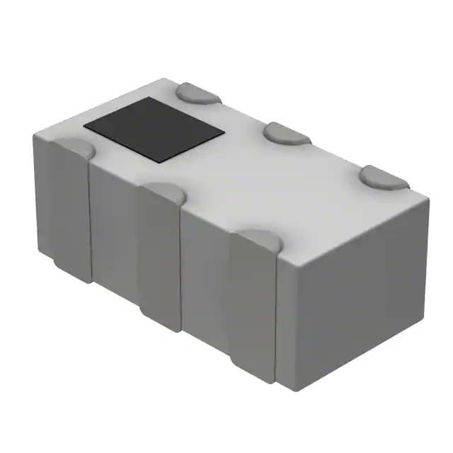
Package: SP5 - industry-standard 4-pin surface-mount package (0.125" × 0.125", 3.18 mm × 3.18 mm) with gull-wing leads, RoHS-compliant and lead-free.
| Pin/Terminal | Circuit Role | Design Meaning |
|---|---|---|
| 1 - PRIMARY DOT | Unbalanced Input (Port 1) | Dot-marked primary terminal; connects to RF source (e.g., LNA output or PA driver) |
| 2 - PRIMARY | Primary Ground Reference | Ground return for unbalanced side; must be low-inductance connection to system ground plane |
| 3 - SECONDARY DOT | Balanced Output (Port 3) | Dot-marked differential output; paired with Pin 4 to deliver 180° phase-inverted signal |
| 4 - SECONDARY | Balanced Output (Port 2) | Non-dot differential output; completes 180° balanced pair with Pin 3 for mixer or ADC interface |
Key Features
| Feature | Design Value |
|---|---|
| Transmission-line balun architecture | Enables broadband performance without ferrite cores or discrete matching, ensuring stable phase/amplitude response across 45–1200 MHz |
| 75 Ω characteristic impedance | Directly interfaces CATV and broadcast RF systems without impedance transformation, reducing component count and layout complexity |
| ≤1.5 dB amplitude balance | Minimizes common-mode noise coupling in differential receivers, improving dynamic range by up to 3 dB in I/Q demodulators |
| SP5 SMT package | Compatible with standard reflow profiles and AOI inspection; supports high-volume automated placement in RF module production |
| RoHS-compliant & lead-free | Fulfills EU Directive 2011/65/EU and 2015/863/EU requirements for hazardous substance restrictions in commercial and industrial equipment |
Applications
| CATV Distribution Amplifier | Wireless Infrastructure Transceiver |
|---|---|
Use Scenario: Signal splitting and amplification in multi-dwelling unit (MDU) coaxial distribution networks operating across 5–1218 MHz. IC Role / Device Role / Timing Role: Balun interface between single-ended GaAs MMIC driver and balanced push-pull amplifier stage. Use Value: Maintains 75 Ω system match and ≤0.8 dB loss across full CATV band, enabling flat gain response and reduced intermodulation distortion. | Use Scenario: I/Q signal conditioning in 4G/5G small-cell base station transceivers supporting 700 MHz–3.8 GHz bands. IC Role / Device Role / Timing Role: Unbalanced-to-balanced conversion for DAC output driving quadrature mixer LO path. Use Value: Achieves ≤10° phase imbalance and ≤1.5 dB amplitude imbalance, directly supporting <−60 dBc image rejection in transmit chain. |
| DOCSIS 4.0 Node RF Front-End | FM/DTV Broadcast Receiver Tuner |
Use Scenario: Upstream channel aggregation in full-duplex DOCSIS 4.0 cable modems requiring simultaneous 5–204 MHz upstream transmission. IC Role / Device Role / Timing Role: Balun between upstream PA and diplexer input, providing common-mode rejection for noise-sensitive upstream paths. Use Value: Delivers ≥20 dB input return loss and 2 W power handling, enabling robust upstream signal integrity under burst-mode operation. | Use Scenario: Antenna interface in terrestrial digital TV (DVB-T/T2) and FM radio tuners operating from 47–862 MHz. IC Role / Device Role / Timing Role: Impedance-matched balun between 75 Ω coaxial antenna feed and balanced tuner IC input. Use Value: Eliminates need for discrete matching components while sustaining >35 dB adjacent-channel rejection via precise amplitude/phase tracking. |
Equivalent & Alternatives
The following parts are listed as comparable options for similar RF balun applications.
| Alternative Part | Technical Difference | Application Difference | Selection Advice |
|---|---|---|---|
| Mini-Circuits ADT1-1WT | 50 Ω impedance, 0.05–500 MHz bandwidth, higher insertion loss (0.9 dB typ. @ 500 MHz) | Optimized for lab test equipment and 50 Ω wireless prototyping, not CATV 75 Ω systems | Select only if system uses 50 Ω architecture and operates below 500 MHz |
| TDK TCM1-83X+ | 75 Ω, 5–1000 MHz, ±15° phase balance, larger 0.156" × 0.156" footprint | Suitable for legacy CATV designs with relaxed phase tolerance and available board area | Choose when board space permits larger package and ±15° phase error is acceptable |
Compared with ADT1-1WT and TCM1-83X+, the RFXF0009H-TR13 uniquely combines 75 Ω impedance, 1200 MHz bandwidth, and ±10° phase balance in the compact SP5 package-making it optimal for space-constrained, high-performance CATV and broadband wireless front-ends requiring strict I/Q fidelity.
Availability
RFXF0009H-TR13 is available at Aetrix Electronics and suitable for CATV node upgrades, wireless small-cell transceivers, DOCSIS 4.0 modems, and broadcast tuner modules requiring stable component supply and RoHS-compliant SMT transformers.
Supply support for RFXF0009H-TR13 includes scheduled delivery planning, volume procurement assistance, BOM continuity management, traceable sourcing, and lifecycle availability coordination for OEM customers, industrial embedded developers, connected-device designers, and electronics production programs.
Manufacturer
Qorvo is a U.S.-based semiconductor company specializing in RF solutions for defense, infrastructure, and mobile markets, with leadership in GaAs, GaN, and BAW technologies.
The RFXF0009H-TR13 belongs to Qorvo's passive RF transformer product line, engineered specifically for broadband 75 Ω signal routing in cable, broadcast, and wireless infrastructure applications where size, reliability, and phase accuracy are critical.
FAQ
What is the maximum RF power rating for RFXF0009H-TR13?
The RFXF0009H-TR13 has an absolute maximum RF power rating of 2 W, validated over its full −40°C to +100°C operating temperature range. This rating supports continuous-wave operation in CATV line drivers and wireless infrastructure power amplifier output stages without thermal degradation. Derating is not required below 100°C ambient, and the device remains within specification up to its storage limit of 100°C.
Does RFXF0009H-TR13 require external DC blocking or biasing components?
No, the RFXF0009H-TR13 is a passive transmission-line transformer with no internal active elements or DC path requirements. It operates transparently across its 45–1200 MHz band without DC blocking capacitors or bias tees. The device supports both AC-coupled and DC-coupled signal paths, provided external circuitry maintains proper RF grounding at Pin 2 (PRIMARY) and avoids DC shorts across the secondary terminals (Pins 3 and 4).
Is RFXF0009H-TR13 compatible with lead-free reflow soldering processes?
Yes, the RFXF0009H-TR13 is fully compatible with standard lead-free reflow profiles, including JEDEC J-STD-020D-compliant peak temperatures up to 260°C. Its SP5 package uses matte tin-plated gull-wing leads and meets RoHS Directive 2011/65/EU and 2015/863/EU requirements. No special pre-bake or moisture sensitivity handling is required prior to assembly.
What does the "DOT" marking indicate on RFXF0009H-TR13 pins?
The "DOT" marking on Pins 1 (PRIMARY DOT) and 3 (SECONDARY DOT) indicates polarity alignment for proper 180° phase inversion. When Pin 1 is driven with a positive-going RF signal, Pin 3 delivers the inverted (180° out-of-phase) output relative to Pin 4. Correct dot-to-dot orientation is essential to maintain intended differential signal polarity in mixer LO or ADC clock paths.
Can RFXF0009H-TR13 be used in 50 Ω systems such as cellular base stations?
The RFXF0009H-TR13 is specified for 75 Ω systems and exhibits degraded return loss and amplitude balance when used in 50 Ω environments. While functional at lower frequencies, its input return loss drops below 15 dB above 200 MHz in 50 Ω configurations. For 50 Ω applications, Qorvo's RFXM0001H or Mini-Circuits ADT1-1WT are better matched alternatives.
RFXF0009H-TR13 Specifications
- Product attributes
- Attribute value
- Manufacturer:
- Qorvo
- Series:
- -
- Package/Case:
- 4-SMD, No Lead
- Packaging:
- Tape & Reel (TR)
- Product Status:
- Active
- Frequency Range:
- 45MHz ~ 1.2GHz
- Impedance - Unbalanced/Balanced:
- 1:1
- Phase Difference:
- 180°
- Insertion Loss (Max):
- 0.8dB
- Return Loss (Min):
- 20dB
- Mounting Type:
- Surface Mount
RFXF0009H-TR13 FAQ
1.How can I place an order for RFXF0009H-TR13 through Aetrix?
Please submit a Request for Quotation (RFQ) for RFXF0009H-TR13 on Aetrix. Our sales agent will provide a competitive quotation and guide you through the order confirmation once you accept the terms.
2.Are the price and stock information for RFXF0009H-TR13 reliable?
The price and inventory of RFXF0009H-TR13 are updated periodically and may fluctuate due to market conditions. Stock and pricing data are typically refreshed every 24 hours. Quotation validity for RFXF0009H-TR13 is usually 5 days.
3.What payment methods are accepted for RFXF0009H-TR13?
We accept Wire Transfer, PayPal, Credit Card, Western Union, MoneyGram, and Escrow for RFXF0009H-TR13 transactions.
Note: Certain payment methods may incur a processing fee.
4.How is shipping managed for RFXF0009H-TR13?
RFXF0009H-TR13 orders can be shipped via leading logistics carriers, including DHL, UPS, FedEx, TNT, or Registered Mail.
Once your RFXF0009H-TR13 order is processed, you will receive an email with the shipment details and tracking number.
Note: Tracking information may take up to 24 hours to appear. Express delivery typically takes 3–5 business days.
5.How can I obtain technical support or documentation for RFXF0009H-TR13?
For technical support, including RFXF0009H-TR13 datasheets, pinout diagrams, or application guidance, please contact our engineering support team. They can provide detailed documentation and assistance for your RFXF0009H-TR13 requirements.
6.How does Aetrix verify that RFXF0009H-TR13 is sourced from the original manufacturer or authorized distributors?
All RFXF0009H-TR13 products on Aetrix are procured from qualified distributors and authorized channels. Our dedicated quality assurance team conducts strict verification, including traceability checks and, if necessary, third-party testing. This ensures that RFXF0009H-TR13 meets industry standards.
7.What is the process for return or replacement of RFXF0009H-TR13?
All RFXF0009H-TR13 units undergo pre-shipment inspection (PSI). If there is an issue with RFXF0009H-TR13, returns or replacements are accepted under the following conditions:
1.Quantity discrepancies, incorrect items, or visible external defects (such as breakage or corrosion), acknowledged by Aetrix.
2.The issue is reported within 90 days of delivery.
3.The RFXF0009H-TR13 part is unused and in its original packaging.
Return procedure for RFXF0009H-TR13:
1.Submit a request within 90 days.
2.Obtain a Return Material Authorization (RMA) from Aetrix.
RFXF0009H-TR13 Tags

-
2450BL15B0100001E
Johanson Technology Inc.

-
0900BL15D0050001E
Johanson Technology Inc.

-
0900PC16J0042001E
Johanson Technology Inc.

-
2450BM15A0002001E
Johanson Technology Inc.

-
2450BM14G0011001T
Johanson Technology Inc.

-
BD0810N50100AHF
TTM Technologies, Inc.

-
1720BL15B0050001E
Johanson Technology Inc.

-
0900PC15A0036001E
Johanson Technology Inc.

-
0868BM15C0001001E
Johanson Technology Inc.

-
0915BM15A0001001E
Johanson Technology Inc.
-
HHM1776B3
TDK Corporation

-
2450BM14E0003001T
Johanson Technology Inc.
Tech Hub

Comparator circuit design covering voltage thresholds, input limits, open-collector outputs, LM393 wiring, op-amp differences, hysteresis, timing, window detection and practical fault diagnosis.
Schmitt triggers use separate rising and falling thresholds to stabilize slow or noisy signals. This guide covers hysteresis, 74HC14 and 74HCT14 selection, comparator calculations, RC oscillators and p…
Counterfeit components can hide behind convincing markings and passing basic function tests. This engineering reference covers source traceability, external inspection, X-ray, XRF, electrical testing, …
A practical engineering and sourcing framework covering lifecycle verification, lifetime-buy calculations, replacement qualification, supplier checks and counterfeit-risk controls.
TTL and CMOS logic families differ in thresholds, loading, output drive, power and timing. This engineering guide compares 74HC and 74HCT, calculates noise margins and checks 3.3 V/5 V compatibility.
A practical engineering guide to 3.3V and 5V logic compatibility, input thresholds, resistor dividers, translator ICs, MOSFET level shifting, I2C pull-ups, timing limits and power-sequencing risks.
The 74HC595 uses push-pull logic outputs, while the TPIC6B595 uses 50 V open-drain DMOS sinks for higher-power loads. This guide compares timing, current limits, 3.3 V interfacing, load wiring, thermal…
The 74HC595 converts serial data into eight stable parallel outputs. This guide covers pin functions, shift and storage timing, OE and MR behavior, drive-current limits, cascading, voltage compatibilit…
A technical comparison of level-sensitive latches and edge-triggered flip-flops, covering timing windows, setup and hold limits, master–slave operation, time borrowing, race-through, HDL inference and…
A D latch stores one bit while Enable controls when data can pass. This reference covers gate-level operation, truth tables, transparency, setup and hold timing, LE versus OE, common ICs and practical …









