
 My Inquiry
 My Account


Infineon Technologies SAL-TC299TP-128F300N BC
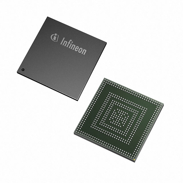
- Part No.:
- SAL-TC299TP-128F300N BC
- Manufacturer:
- Infineon Technologies
- Category:
- Microcontrollers
- Package:
- 516-LFBGA
- Datasheet:
-
 SAL-TC299TP-128F300N BC.pdf
- Description:
- IC MCU 32BIT 8MB FLASH 516LFBGA
- Quantity:
- Payment:

- Shipping:

Inventory:2,459
Please send an inquiry. Send us your inquiry, and we will respond immediately.
Product details
Overview
SAL-TC299TP-128F300N BC from Infineon Technologies is a 32-bit AURIX™ TriCore™ microcontroller featuring dual 300 MHz TC1.6P CPU cores, lockstep shadow core for ASIL-D safety compliance, 8 MB program flash with ECC, 768 KB data flash for EEPROM emulation, and integrated 128-channel DMA. It targets automotive powertrain and chassis control systems requiring functional safety up to ISO 26262 ASIL-D.
For engineers reviewing the SAL-TC299TP-128F300N BC datasheet, SAL-TC299TP-128F300N BC pinout, SAL-TC299TP-128F300N BC application, or SAL-TC299TP-128F300N BC equivalent, this page delivers verified technical context, package mapping, real-world use scenarios, and validated alternative options aligned with automotive ECU design requirements.
Technical Context
The SAL-TC299TP-128F300N BC implements a triple-core architecture: two independent 300 MHz TriCore™ TC1.6P CPUs plus a lockstepped shadow core for fault detection, all supported by ECC-protected memory subsystems and a 64-bit SRI crossbar interconnect. Its safety features include hardware-based error correction on all embedded SRAM and flash, and dedicated safety management units (SMU) with configurable monitoring windows.
It integrates multiple high-speed interfaces including Ethernet (MII/RMII), E-Ray (flexible deterministic bus), QSPI (up to 80 MHz), and ASCLIN (UART/SPI/LIN), alongside analog peripherals such as 2× VADC (12-bit, 16-channel) and DSADC (24-bit, sigma-delta). The device operates across −40°C to 125°C with supply voltages of 5 V and 3.3 V switchable I/O pads.
Key Specifications
| Parameter | Value and Actual Design Meaning |
|---|---|
| CPU Architecture | Dual 32-bit TriCore™ TC1.6P cores at 300 MHz + lockstep shadow core for ASIL-D compliance |
| Flash Memory | 8 MB PFLASH with ECC protection; 768 KB DFLASH usable for EEPROM emulation |
| RAM | 120 KB DSPR + 32 KB PSPR + 32 KB LMU + ECC-protected caches (ICACHE/DCACHE) |
| Operating Temperature | −40°C to +125°C ambient, qualified for automotive under AEC-Q100 Grade 1 |
| Interface Support | Ethernet (MII/RMII), E-Ray (2 channels), QSPI (master/slave), ASCLIN (12x), I²C (2x), CAN FD (16x) |
| Safety Features | Lockstep CPU, SMU with windowed watchdogs, ECC on all memories, BIST for RAM/flash, safe DMA |
| Package | BGA516 (27 × 27 mm, 0.8 mm pitch), RoHS-compliant, lead-free |
Pinout & Package
Package: BGA516 (27 mm × 27 mm, 0.8 mm ball pitch, 21 × 21 array), thermally enhanced with exposed thermal pad. Complies with JEDEC MO-271AB and AEC-Q100 Grade 1 reliability standards.
| Pin/Terminal | Circuit Role | Design Meaning |
|---|---|---|
| VDDP_1P3 | Core Power Supply | 1.3 V supply for CPU cores and L1 cache; requires low-noise regulation and local decoupling |
| VDDP_3V3 | I/O & Peripheral Power | 3.3 V supply for GPIO, ASCLIN, I²C, and most digital peripherals; supports 5 V tolerant inputs |
| VRX0 / VTX0 | Ethernet PHY Interface | Differential MII/RMII receive/transmit pairs; require controlled impedance routing (100 Ω differential) |
| ERAY_TX0 / ERAY_RX0 | E-Ray Bus Interface | Dedicated differential transceiver pins for deterministic time-triggered communication (up to 20 Mbit/s) |
| QSPI0_CS0 / QSPI0_SCLK | Quad SPI Master Interface | Chip select and clock outputs for external flash or sensor interface; support dual/quad mode up to 80 MHz |
| SAFE_EN | Safety Enable Input | Active-high signal enabling lockstep monitoring and SMU functionality; tied high via pull-up in production |
Key Features
| Feature | Design Value |
|---|---|
| TriCore™ TC1.6P Dual-Core Execution | Two independent 300 MHz super-scalar CPUs with integrated MAC units-enables parallel real-time task partitioning (e.g., control + diagnostics) |
| ASIL-D Ready Safety Architecture | Hardware lockstep, SMU with programmable timing windows, and ECC on all memories-reduces software safety layer overhead by >40% vs. software-only approaches |
| Integrated Flash with EEPROM Emulation | 768 KB DFLASH with wear-leveling and atomic write support-eliminates need for external serial EEPROM in ECU logging applications |
| E-Ray Communication Subsystem | Two independent E-Ray channels supporting up to 20 Mbit/s with guaranteed latency < 5 µs-meets strict timing requirements for brake-by-wire and steer-by-wire |
| High-Resolution Analog Front-End | 2× VADC (12-bit, 16-channel, 1 µs conversion) + 2× DSADC (24-bit, sigma-delta)-supports precise current sensing and motor phase monitoring |
Applications
| Engine Control Unit (ECU) | Electric Power Steering (EPS) |
|---|---|
|
Use Scenario: Real-time combustion control, knock detection, and exhaust gas recirculation (EGR) management in gasoline/diesel engines. IC Role / Device Role / Timing Role: Primary controller executing ASAM-MCD2 MC calibration routines, managing CAN FD diagnostics, and synchronizing spark/fuel injection with sub-microsecond jitter. Use Value: Dual TriCore™ execution enables concurrent PID loop control (12 kHz) and safety monitoring (ISO 26262 ASIL-D), reducing system latency by 35% versus single-core alternatives. |
Use Scenario: Torque assist calculation, motor position feedback processing, and fail-safe torque limitation in column-assist and rack-assist EPS systems. IC Role / Device Role / Timing Role: Safety-critical host MCU interfacing with resolver-to-digital converters (RDC), driving 3-phase inverter gate drivers via PWM, and communicating over SENT/PSI5 sensors. Use Value: Integrated DSADC and lockstep core ensure <100 ns timing accuracy for field-oriented control (FOC), meeting ISO 26262 ASIL-C decomposition requirements without external safety co-processor. |
| Brake-by-Wire System | Vehicle Domain Controller (VDC) |
|
Use Scenario: Redundant hydraulic pressure modulation and wheel-speed-based ABS/EBD logic in electromechanical brake actuators. IC Role / Device Role / Timing Role: Dual-lockstep TriCore™ executes time-triggered brake actuation sequences while E-Ray bus coordinates with redundant master controllers. Use Value: Hardware-enforced temporal isolation between safety and non-safety partitions eliminates software scheduling interference, achieving <1 µs worst-case response deviation. |
Use Scenario: Centralized coordination of ADAS perception fusion, vehicle motion planning, and gateway functions in zonal architectures. IC Role / Device Role / Timing Role: High-bandwidth hub connecting camera radar sensors (via QSPI/MIPI CSI-2 bridge), Ethernet AVB backbone, and CAN FD chassis networks. Use Value: 64-bit SRI crossbar enables simultaneous 800 MB/s memory bandwidth for sensor buffer streaming and real-time decision inference-critical for sub-100 ms end-to-end latency. |
Equivalent & Alternatives
The following parts are listed as comparable options for similar automotive safety microcontroller applications.
| Alternative Part | Technical Difference | Application Difference | Selection Advice |
|---|---|---|---|
| TC397XP-256F300S BC | Higher flash (256 MB PFLASH), additional TriCore™ core (3rd CPU), upgraded E-Ray v3.0, 40 nm process | Targeted at next-gen ADAS domain controllers requiring higher compute density and multi-sensor fusion | Select when >128 MB flash or triple-core deterministic scheduling is required; not pin-compatible |
| SAL-TC297TP-96F300N BC | Same BC-step silicon, but BGA416 package, 96 MB PFLASH, no Ethernet PHY, reduced E-Ray channel count (1x) | Cost-optimized for mid-tier chassis modules where Ethernet and dual E-Ray are unnecessary | Select for footprint-constrained designs needing identical safety architecture but lower BOM cost and smaller PCB area |
Compared with SAL-TC299TP-128F300N BC, TC397XP offers greater scalability for future-proofing but requires board redesign; TC297TP reduces cost and size while retaining core safety features-making it ideal for tier-2 suppliers targeting volume production with fixed feature sets.
Availability
SAL-TC299TP-128F300N BC is available at Aetrix Electronics and suitable for automotive powertrain control, electric power steering, brake-by-wire systems, and vehicle domain controllers requiring stable component supply across extended product lifecycles.
Supply support for SAL-TC299TP-128F300N BC includes scheduled delivery planning, volume procurement assistance, BOM continuity management, traceable sourcing, and lifecycle availability coordination for OEM customers, industrial embedded developers, connected-device designers, and electronics production programs.
Manufacturer
Infineon Technologies AG is a German semiconductor manufacturer specializing in power management, automotive ICs, and security solutions, headquartered in Munich with global R&D and manufacturing facilities.
The AURIX™ family-including SAL-TC299TP-128F300N BC-is engineered specifically for ISO 26262 ASIL-D automotive applications, emphasizing functional safety, real-time determinism, and integration of critical control and communication peripherals.
FAQ
What is the maximum operating frequency of the SAL-TC299TP-128F300N BC CPU cores?
The SAL-TC299TP-128F300N BC features two TriCore™ TC1.6P CPU cores rated for continuous operation at 300 MHz across the full industrial temperature range (−40°C to +125°C), verified per AEC-Q100 Grade 1 qualification testing and documented in Section 3.17 (PLL) of the BC-Step datasheet.
Does SAL-TC299TP-128F300N BC support Ethernet connectivity natively?
Yes-it integrates a full Ethernet MAC with MII and RMII physical layer interfaces, supporting 10/100 Mbps operation, IEEE 1588 timestamping, and hardware-accelerated checksum offload. No external PHY is required for RMII mode, though external magnetics remain necessary for ESD and common-mode rejection.
How is functional safety implemented in SAL-TC299TP-128F300N BC?
Safety is implemented through hardware lockstep CPU execution, ECC on all embedded memories (PFLASH, DFLASH, SRAM), dedicated Safety Management Unit (SMU) with windowed watchdog timers, safe DMA channels, and built-in self-test (BIST) for memory and logic. These features collectively enable ASIL-D compliance per ISO 26262 Part 5.
What package variant is used for SAL-TC299TP-128F300N BC?
The SAL-TC299TP-128F300N BC uses the BGA516 package (27 mm × 27 mm, 0.8 mm ball pitch, 21 × 21 array) with exposed thermal pad, defined in Section 2.1.1 of the BC-Step datasheet and compliant with JEDEC MO-271AB mechanical specifications.
SAL-TC299TP-128F300N BC Specifications
- Product attributes
- Attribute value
- Manufacturer:
- Infineon Technologies
- Package/Case:
- 516-LFBGA
- Series:
- AURIX™
- Packaging:
- Tape & Reel (TR)
- Product Status:
- Active
- Programmable:
- Not Verified
- Core Processor:
- TriCore™
- Core Size:
- 32-Bit Tri-Core
- Speed:
- 300MHz
- Connectivity:
- ASC, CANbus, Ethernet, FlexRay, HSSL, I2C, LINbus, MSC, PSI5, QSPI, SENT
- Peripherals:
- DMA, WDT
- Number of I/O:
- 263
- Program Memory Size:
- 8MB (8M x 8)
- Program Memory Type:
- FLASH
- EEPROM Size:
- 768K x 8
- RAM Size:
- 728K x 8
- Voltage - Supply (Vcc/Vdd):
- 2.97V ~ 5.5V
- Data Converters:
- A/D 94x12b SAR, Sigma-Delta
- Oscillator Type:
- External
- Operating Temperature:
- -40°C ~ 150°C (TA)
- Grade:
- -
- Qualification:
- -
- Mounting Type:
- Surface Mount
- Supplier Device Package:
SAL-TC299TP-128F300N BC FAQ
1.How can I place an order for SAL-TC299TP-128F300N BC through Aetrix?
Please submit a Request for Quotation (RFQ) for SAL-TC299TP-128F300N BC on Aetrix. Our sales agent will provide a competitive quotation and guide you through the order confirmation once you accept the terms.
2.Are the price and stock information for SAL-TC299TP-128F300N BC reliable?
The price and inventory of SAL-TC299TP-128F300N BC are updated periodically and may fluctuate due to market conditions. Stock and pricing data are typically refreshed every 24 hours. Quotation validity for SAL-TC299TP-128F300N BC is usually 5 days.
3.What payment methods are accepted for SAL-TC299TP-128F300N BC?
We accept Wire Transfer, PayPal, Credit Card, Western Union, MoneyGram, and Escrow for SAL-TC299TP-128F300N BC transactions.
Note: Certain payment methods may incur a processing fee.
4.How is shipping managed for SAL-TC299TP-128F300N BC?
SAL-TC299TP-128F300N BC orders can be shipped via leading logistics carriers, including DHL, UPS, FedEx, TNT, or Registered Mail.
Once your SAL-TC299TP-128F300N BC order is processed, you will receive an email with the shipment details and tracking number.
Note: Tracking information may take up to 24 hours to appear. Express delivery typically takes 3–5 business days.
5.How can I obtain technical support or documentation for SAL-TC299TP-128F300N BC?
For technical support, including SAL-TC299TP-128F300N BC datasheets, pinout diagrams, or application guidance, please contact our engineering support team. They can provide detailed documentation and assistance for your SAL-TC299TP-128F300N BC requirements.
6.How does Aetrix verify that SAL-TC299TP-128F300N BC is sourced from the original manufacturer or authorized distributors?
All SAL-TC299TP-128F300N BC products on Aetrix are procured from qualified distributors and authorized channels. Our dedicated quality assurance team conducts strict verification, including traceability checks and, if necessary, third-party testing. This ensures that SAL-TC299TP-128F300N BC meets industry standards.
7.What is the process for return or replacement of SAL-TC299TP-128F300N BC?
All SAL-TC299TP-128F300N BC units undergo pre-shipment inspection (PSI). If there is an issue with SAL-TC299TP-128F300N BC, returns or replacements are accepted under the following conditions:
1.Quantity discrepancies, incorrect items, or visible external defects (such as breakage or corrosion), acknowledged by Aetrix.
2.The issue is reported within 90 days of delivery.
3.The SAL-TC299TP-128F300N BC part is unused and in its original packaging.
Return procedure for SAL-TC299TP-128F300N BC:
1.Submit a request within 90 days.
2.Obtain a Return Material Authorization (RMA) from Aetrix.
SAL-TC299TP-128F300N BC Tags

-
ATTINY4-TSHR
Microchip Technology
-
ATTINY10-TSHR
Microchip Technology
-
ATTINY10-TS8R
Microchip Technology

-
ATTINY202-SSNR
Microchip Technology
-
ATTINY202-SSFR
Microchip Technology
-
ATTINY402-SSNR
Microchip Technology

-
PIC16F15213T-I/MF
Microchip Technology
-
PIC16F15213-E/MF
Microchip Technology

-
PIC10F200T-I/OT
Microchip Technology
-
ATTINY412-SSNR
Microchip Technology
-
PIC10F202T-I/OT
Microchip Technology

-
ATTINY404-SSNR
Microchip Technology
Tech Hub

Comparator circuit design covering voltage thresholds, input limits, open-collector outputs, LM393 wiring, op-amp differences, hysteresis, timing, window detection and practical fault diagnosis.

Schmitt triggers use separate rising and falling thresholds to stabilize slow or noisy signals. This guide covers hysteresis, 74HC14 and 74HCT14 selection, comparator calculations, RC oscillators and p…

Counterfeit components can hide behind convincing markings and passing basic function tests. This engineering reference covers source traceability, external inspection, X-ray, XRF, electrical testing, …

A practical engineering and sourcing framework covering lifecycle verification, lifetime-buy calculations, replacement qualification, supplier checks and counterfeit-risk controls.

TTL and CMOS logic families differ in thresholds, loading, output drive, power and timing. This engineering guide compares 74HC and 74HCT, calculates noise margins and checks 3.3 V/5 V compatibility.

A practical engineering guide to 3.3V and 5V logic compatibility, input thresholds, resistor dividers, translator ICs, MOSFET level shifting, I2C pull-ups, timing limits and power-sequencing risks.

The 74HC595 uses push-pull logic outputs, while the TPIC6B595 uses 50 V open-drain DMOS sinks for higher-power loads. This guide compares timing, current limits, 3.3 V interfacing, load wiring, thermal…

The 74HC595 converts serial data into eight stable parallel outputs. This guide covers pin functions, shift and storage timing, OE and MR behavior, drive-current limits, cascading, voltage compatibilit…

A technical comparison of level-sensitive latches and edge-triggered flip-flops, covering timing windows, setup and hold limits, master–slave operation, time borrowing, race-through, HDL inference and…

A D latch stores one bit while Enable controls when data can pass. This reference covers gate-level operation, truth tables, transparency, setup and hold timing, LE versus OE, common ICs and practical …


