Send an Inquiry

To receive a quote for your project, please fill in the following information, and we’ll get back to you promptly.

Name*
Company*
Email Address*
Phone/WhatsApp
Part Number*
Quantity*
Message
Submit Inventory List

Please fill in the following information, and we’ll get back to you promptly.

Name*
Company*
Email Address*
Phone/WhatsApp
Upload My List
Message

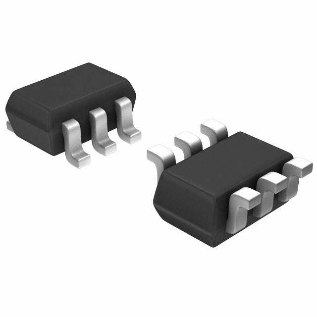
Vishay Siliconix SI1865DDL-T1-BE3

Part No.:
SI1865DDL-T1-BE3
Manufacturer:
Vishay Siliconix
Category:
Power Distribution Switches, Load Drivers
Package:
6-TSSOP, SC-88, SOT-363
Datasheet:
AetrixSI1865DDL-T1-BE3.pdf
Description:
IC PWR SWITCH P-CHAN 1:1 SC70-6
Quantity:
Payment:
Payment
Shipping:
Shipping

Inventory:2,699

Please send an inquiry. Send us your inquiry, and we will respond immediately.

Part Number
Quantity*
Price
Name*
Company
Email*
Comments

Product details

Overview

SI1865DDL-T1-BE3 from Vishay Siliconix is a dual-MOSFET load switch with integrated level-shift functionality, combining a p-channel TrenchFET (RDS(on) = 0.200 Ω at VIN = 4.5 V) and an n-channel MOSFET in a single SC-70-6 package. It operates from 1.8 V to 12 V input, accepts 1.5 V to 8 V logic-level control, delivers ±1.1 A continuous load current, and features 2000 V HBM ESD protection on the ON/OFF pin - ideal for high-side power management in space-constrained portable devices.

For engineers reviewing the SI1865DDL-T1-BE3 datasheet, SI1865DDL-T1-BE3 pinout, SI1865DDL-T1-BE3 application, or SI1865DDL-T1-BE3 equivalent, this device enables compact, slew-rate-adjustable load switching with minimal external components - critical for battery-powered consumer electronics requiring precise inrush control and low-voltage logic compatibility.

Technical Context

The SI1865DDL-T1-BE3 integrates two complementary MOSFETs: a low-RDS(on) p-channel device optimized as a high-side load switch, and an n-channel device configured as a level-shifter to drive the p-channel gate using low-voltage logic (≥1.5 V). Its operation relies on external R2 (0–100 kΩ) and optional C1 (1000 pF) to set slew rate, enabling tailored rise/fall times for different capacitive loads.

Thermal performance is defined by RthJA = 350 °C/W (max) and RthJF = 300 °C/W (max), with absolute maximum ratings including VIN = 12 V, VON/OFF = 8 V, and TJ = –55 to +150 °C. The device supports pulsed load currents up to ±5 A under specified pulse conditions.

Key Specifications

Parameter Value and Actual Design Meaning
VDS Rating12 V - supports input rails up to 12 V without breakdown
RDS(on) @ 4.5 V0.200 Ω - enables <110 mV dropout at 1.1 A, minimizing power loss
Logic Input Range1.5 V to 8 V - interfaces directly with 1.8 V, 2.5 V, 3.3 V, and 5 V microcontrollers
Continuous Load Current±1.1 A - sufficient for USB peripherals, display backlights, and sensor modules
ESD Protection2000 V HBM on ON/OFF pin - enhances robustness in handheld assembly and end-use environments
PackageSC-70-6 - 2.0 × 2.1 mm footprint, 0.95 mm height, suitable for ultra-thin portable PCBs
Slew Rate ControlExternally adjustable via R2 (0–100 kΩ) and C1 - prevents voltage droop and EMI during hot-swap events

Pinout & Package

SI1865DDL-T1-BE3 is housed in a lead (Pb)-free, halogen-free SC-70-6 package (JEDEC MO-203AA), with 0.65 mm pitch, 2.0 mm × 2.1 mm body, and 0.95 mm max height. Pin 1 is marked with a dot; top view orientation matches standard SC-70 pin numbering.

Pin/Terminal Circuit Role Design Meaning
1ON/OFF (n-ch gate)Logic-level input controlling n-channel MOSFET; drives p-channel gate via internal connection
2, 3Source of n-channel (S2)Connected internally to GND; provides reference for level-shift circuit
4Drain of p-channel (D1)High-side switch output - connects to load; carries full load current
5Source of p-channel (S1)Input supply rail (VIN); must be decoupled near device for stability
6Drain of n-channel (D2)Internally connected to p-channel gate; forms active level-shift stage

Key Features

Feature Design Value
TrenchFET® p-channel technologyDelivers 0.200 Ω RDS(on) at 4.5 V, reducing conduction loss vs. planar alternatives
Integrated level-shift architectureEliminates need for discrete level-shifter IC or resistor-divider network, saving ≥3 BOM items
Adjustable slew-rate controlExternal R2/C1 sets turn-on/turn-off timing to match load capacitance and prevent bus collapse
1.5 V logic-compatible inputEnables direct interface with modern ultra-low-voltage MCUs (e.g., ARM Cortex-M0+) without level translators
2000 V HBM ESD protectionMeets IEC 61000-4-2 Level 4 requirements for handheld product handling and field reliability

Applications

Smartphone Power Rail Switching USB OTG Peripheral Enable

Use Scenario: Enabling/disabling camera module or audio codec power rail during sleep/wake transitions.

IC Role / Device Role / Timing Role: High-side load switch with controlled slew to limit inrush into 100–500 µF local bulk capacitance.

Use Value: Prevents system voltage droop below 2.8 V during hot-plug, avoiding brown-out resets in baseband processors.

Use Scenario: Activating USB OTG accessory power only when host negotiation completes.

IC Role / Device Role / Timing Role: Logic-controlled power gate with 1.8 V compatible enable signal from USB controller.

Use Value: Ensures VBUS is not asserted prematurely, meeting USB 2.0 enumeration timing and power budget constraints.

Wearable Sensor Hub Power Management Bluetooth LE Module Enable

Use Scenario: Sequencing power to inertial measurement unit (IMU) and environmental sensors in fitness trackers.

IC Role / Device Role / Timing Role: Dual-rail switch enabling independent control of analog and digital sensor domains.

Use Value: Reduces quiescent current to <1 µA in off-state while supporting fast (<10 µs) wake-up response.

Use Scenario: Turning on Bluetooth LE radio only during advertising or connection intervals.

IC Role / Device Role / Timing Role: Low-RDS(on) load switch driven by GPIO from BLE SoC operating at 1.8 V logic.

Use Value: Achieves <50 mΩ effective on-resistance at 1.8 V VIN, minimizing voltage drop across 300 mA peak transmit current.

Equivalent & Alternatives

The following parts are listed as comparable options for similar load-switch-with-level-shift applications.

Alternative Part Technical Difference Application Difference Selection Advice
Si1867DDL-T1-BE3RDS(on) = 0.145 Ω @ 4.5 V; same SC-70-6 package and pinoutBetter efficiency at higher currents (>800 mA); identical control interface and thermal profileSelect when lower conduction loss is prioritized over cost sensitivity
TPS22967DSGRSingle-channel, 12 V, 2 A load switch with integrated slew control; 1.8 V logic compatible; WSON-8 packageNo level-shift function - requires external logic translation for sub-1.8 V controllers; larger footprintChoose when higher current rating and factory-programmable slew are required, and board area permits 2.0 × 2.0 mm WSON

Compared with SI1865DDL-T1-BE3, Si1867DDL-T1-BE3 offers lower RDS(on) but identical integration and layout; TPS22967DSGR trades level-shift capability for higher current and programmability, requiring PCB redesign due to different package and pin count.

Availability

SI1865DDL-T1-BE3 is available at Aetrix Electronics and suitable for smartphone power sequencing, wearable sensor hub enablement, and USB OTG peripheral control requiring stable component supply, consistent lead-time visibility, and long-term industrial lifecycle support.

Supply support for SI1865DDL-T1-BE3 includes scheduled delivery planning, volume procurement assistance, BOM continuity management, traceable sourcing, and lifecycle availability coordination for OEM customers, industrial embedded developers, connected-device designers, and electronics production programs.

Manufacturer

Vishay Siliconix is a global leader in discrete semiconductors, specializing in MOSFETs, diodes, optoelectronics, and passive components with emphasis on power efficiency and reliability.

The SI1865DDL-T1-BE3 belongs to Vishay's TrenchFET® Load Switch family, engineered specifically for space-constrained, battery-operated consumer electronics needing integrated level-shift and adjustable slew-rate control.

FAQ

What is the maximum input voltage the SI1865DDL-T1-BE3 can handle?

The SI1865DDL-T1-BE3 has an absolute maximum input voltage (VIN) rating of 12 V, as specified in its Absolute Maximum Ratings table. Operation above this voltage risks permanent damage. For reliable long-term use, design margins should keep VIN ≤ 10.8 V under worst-case conditions. The SI1865DDL-T1-BE3 maintains stable RDS(on) performance across its full 1.8 V to 12 V operating range.

Can the SI1865DDL-T1-BE3 be used with a 1.2 V logic controller?

No - the SI1865DDL-T1-BE3 requires a minimum ON/OFF input voltage of 1.5 V to ensure proper n-channel MOSFET turn-on and reliable p-channel gate drive. A 1.2 V controller falls below the guaranteed functional threshold and may result in incomplete switching or increased RDS(on). For 1.2 V systems, external level translation or a different load switch such as the NX3P185UK is required. The SI1865DDL-T1-BE3 is validated for 1.5 V to 8 V logic compatibility.

How is slew rate adjusted on the SI1865DDL-T1-BE3?

Slew rate on the SI1865DDL-T1-BE3 is set externally using resistor R2 between pins 1 (ON/OFF) and 6 (D2), optionally with capacitor C1 from pin 6 to ground. Typical R2 values range from 0 to 100 kΩ; increasing R2 lengthens turn-on/turn-off times. At VIN = 2.5 V and R1 = 20 kΩ, tr/tf vary from ~1.5 µs (R2 = 0 kΩ) to ~14 µs (R2 = 100 kΩ). The SI1865DDL-T1-BE3 datasheet provides detailed curves for R2 vs. timing across multiple VIN conditions.

Does the SI1865DDL-T1-BE3 include reverse-current blocking?

Yes - the SI1865DDL-T1-BE3 provides inherent reverse-current blocking via its p-channel high-side configuration. When disabled (ON/OFF = low), the p-channel MOSFET's body diode is reverse-biased, preventing current flow from VOUT to VIN. This protects upstream supplies during hot-swap or fault conditions. Reverse leakage is limited to ≤1 µA at VIN = 12 V, ensuring minimal standby drain. The SI1865DDL-T1-BE3 does not require external diodes for this function.

What is the thermal resistance of the SI1865DDL-T1-BE3 in typical PCB layout?

The SI1865DDL-T1-BE3 has a maximum junction-to-ambient thermal resistance (RthJA) of 350 °C/W under standard JEDEC test conditions (single-layer 1 in² copper pad, FR4 board). In a well-designed layout with 2 oz copper, thermal vias under the exposed pad (pins 2/3), and 2 in² of copper pour, RthJA can improve to ~220 °C/W. The SI1865DDL-T1-BE3 junction temperature must remain ≤150 °C; at 1.1 A and 0.200 Ω RDS(on), PD = 242 mW, requiring ≤414 °C/W margin - easily met with basic thermal relief.

SI1865DDL-T1-BE3 Specifications

Product attributes
Attribute value
Manufacturer:
Vishay Siliconix
Package/Case:
6-TSSOP, SC-88, SOT-363
Series:
TrenchFET®
Packaging:
Tape & Reel (TR)
Product Status:
Active
Switch Type:
General Purpose
Number of Outputs:
1
Ratio - Input:Output:
1:1
Output Configuration:
High Side
Output Type:
P-Channel
Interface:
On/Off
Voltage - Load:
1.8V ~ 12V
Voltage - Supply (Vcc/Vdd):
1.5V ~ 8V
Current - Output (Max):
1.1A
Rds On (Typ):
165mOhm
Input Type:
-
Features:
Slew Rate Controlled
Fault Protection:
-
Operating Temperature:
-55°C ~ 150°C (TJ)
Grade:
-
Qualification:
-
Mounting Type:
Surface Mount
Supplier Device Package:
SC-70-6

SI1865DDL-T1-BE3 FAQ

1.How can I place an order for SI1865DDL-T1-BE3 through Aetrix?

Please submit a Request for Quotation (RFQ) for SI1865DDL-T1-BE3 on Aetrix. Our sales agent will provide a competitive quotation and guide you through the order confirmation once you accept the terms.

2.Are the price and stock information for SI1865DDL-T1-BE3 reliable?

The price and inventory of SI1865DDL-T1-BE3 are updated periodically and may fluctuate due to market conditions. Stock and pricing data are typically refreshed every 24 hours. Quotation validity for SI1865DDL-T1-BE3 is usually 5 days.

3.What payment methods are accepted for SI1865DDL-T1-BE3?

We accept Wire Transfer, PayPal, Credit Card, Western Union, MoneyGram, and Escrow for SI1865DDL-T1-BE3 transactions.

Note: Certain payment methods may incur a processing fee.

4.How is shipping managed for SI1865DDL-T1-BE3?

SI1865DDL-T1-BE3 orders can be shipped via leading logistics carriers, including DHL, UPS, FedEx, TNT, or Registered Mail.

Once your SI1865DDL-T1-BE3 order is processed, you will receive an email with the shipment details and tracking number.

Note: Tracking information may take up to 24 hours to appear. Express delivery typically takes 3–5 business days.

5.How can I obtain technical support or documentation for SI1865DDL-T1-BE3?

For technical support, including SI1865DDL-T1-BE3 datasheets, pinout diagrams, or application guidance, please contact our engineering support team. They can provide detailed documentation and assistance for your SI1865DDL-T1-BE3 requirements.

6.How does Aetrix verify that SI1865DDL-T1-BE3 is sourced from the original manufacturer or authorized distributors?

All SI1865DDL-T1-BE3 products on Aetrix are procured from qualified distributors and authorized channels. Our dedicated quality assurance team conducts strict verification, including traceability checks and, if necessary, third-party testing. This ensures that SI1865DDL-T1-BE3 meets industry standards.

7.What is the process for return or replacement of SI1865DDL-T1-BE3?

All SI1865DDL-T1-BE3 units undergo pre-shipment inspection (PSI). If there is an issue with SI1865DDL-T1-BE3, returns or replacements are accepted under the following conditions:

1.Quantity discrepancies, incorrect items, or visible external defects (such as breakage or corrosion), acknowledged by Aetrix.

2.The issue is reported within 90 days of delivery.

3.The SI1865DDL-T1-BE3 part is unused and in its original packaging.

Return procedure for SI1865DDL-T1-BE3:

1.Submit a request within 90 days.

2.Obtain a Return Material Authorization (RMA) from Aetrix.

SI1865DDL-T1-BE3 Tags

  • SI1865DDL-T1-BE3
  • SI1865DDL-T1-BE3 PDF
  • SI1865DDL-T1-BE3 Datasheet
  • SI1865DDL-T1-BE3 Specifications
  • SI1865DDL-T1-BE3 Images
  • Vishay Siliconix
  • Vishay Siliconix SI1865DDL-T1-BE3
  • Buy SI1865DDL-T1-BE3
  • SI1865DDL-T1-BE3 Price
  • SI1865DDL-T1-BE3 Distributor
  • SI1865DDL-T1-BE3 Supplier
  • SI1865DDL-T1-BE3 Wholesale
Related Products
TPS22919DCKR
TPS22919DCKR

Texas Instruments

MIC2091-1YM5-TR
MIC2091-1YM5-TR

Microchip Technology

MIC2090-1YM5-TR
MIC2090-1YM5-TR

Microchip Technology

TPS22995RZFR
TPS22995RZFR

Texas Instruments

TPS22975DSGR
TPS22975DSGR

Texas Instruments

SIP32510DT-T1-GE3
SIP32510DT-T1-GE3

Vishay Siliconix

ULN2003D1013TR
ULN2003D1013TR

STMicroelectronics

MIC2005A-1YM5-TR
MIC2005A-1YM5-TR

Microchip Technology

MIC2005A-1YM6-TR
MIC2005A-1YM6-TR

Microchip Technology

TPS22916BYFPR
TPS22916BYFPR

Texas Instruments

TPS22917DBVR
TPS22917DBVR

Texas Instruments

ULN2003APWR
ULN2003APWR

Texas Instruments

Tech Hub

Search

Search

PRODUCT

PRODUCT

PHONE

PHONE

USER

USER