Send an Inquiry

To receive a quote for your project, please fill in the following information, and we’ll get back to you promptly.

Name*
Company*
Email Address*
Phone/WhatsApp
Part Number*
Quantity*
Message
Submit Inventory List

Please fill in the following information, and we’ll get back to you promptly.

Name*
Company*
Email Address*
Phone/WhatsApp
Upload My List
Message

Vishay Siliconix SI1867DL-T1-E3

Part No.:
SI1867DL-T1-E3
Manufacturer:
Vishay Siliconix
Category:
Power Distribution Switches, Load Drivers
Package:
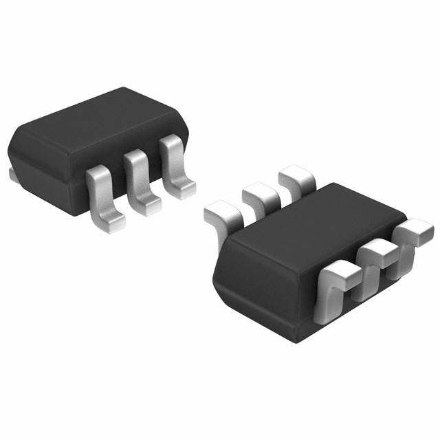
6-TSSOP, SC-88, SOT-363
Datasheet:
AetrixSI1867DL-T1-E3.pdf
Description:
IC PWR SWITCH P-CHAN 1:1 SC70-6
Quantity:
Payment:
Payment
Shipping:
Shipping

Inventory:1,933

Please send an inquiry. Send us your inquiry, and we will respond immediately.

Part Number
Quantity*
Price
Name*
Company
Email*
Comments

Product details

Overview

SI1867DL-T1-E3 from Vishay Siliconix is a dual-MOSFET load switch IC integrating a p-channel TrenchFET (RDS(on) = 0.600 Ω at VIN = 4.5 V) and an n-channel MOSFET for level-shift control, operating from 1.8 V to 8 V input, supporting ±0.6 A continuous load current, and housed in SC70-6 package - used for high-side load switching in space-constrained portable electronics.

For engineers reviewing the SI1867DL-T1-E3 datasheet, SI1867DL-T1-E3 pinout, SI1867DL-T1-E3 application, or SI1867DL-T1-E3 equivalent, key selection considerations include its logic-level compatibility down to 1.5 V, externally adjustable slew rate via R2/C1, integrated ESD protection (2 kV HBM), and thermal resistance (RthJA = 320 °C/W) for low-power battery-operated systems.

Technical Context

The SI1867DL-T1-E3 implements a high-side load switch architecture where the p-channel MOSFET handles main power path conduction while the n-channel MOSFET acts as a gate driver with level-shift capability - enabling direct interface with low-voltage logic (≥1.5 V). Its dual-FET integration eliminates discrete level-shifter components.

Switching behavior is externally programmable: rise/fall times are set by optional R2 (0–100 kΩ) and C1 (1000 pF), allowing tailoring of inrush current for diverse capacitive loads. The device supports operation across -55 °C to +150 °C junction temperature range with guaranteed performance at 25 °C and derated limits at extremes.

Key Specifications

ParameterValue and Actual Design Meaning
Input Voltage Range1.8 V to 8 V - enables use across single-cell Li-ion (2.7–4.2 V), 3.3 V, and 5 V rails without external regulators.
P-Channel RDS(on)0.600 Ω at VIN = 4.5 V, ID = 0.6 A - limits voltage drop to ≤360 mV at full rated load, minimizing power loss and heat generation.
Logic Control Threshold1.5 V to 8 V - ensures reliable turn-on with 1.8 V GPIOs and compatibility with 3.3 V/5 V controllers without level translators.
Continuous Load Current±0.6 A - supports moderate-power peripherals like displays, sensors, or USB ports in portable devices.
Thermal ResistanceRthJA = 320 °C/W - defines maximum power dissipation (0.4 W) under standard FR4 PCB conditions; requires careful layout for sustained loads.
ESD Rating2 kV HBM - provides basic handling robustness during assembly but not system-level ESD immunity; external protection may be needed.

Pinout & Package

SC70-6 package: ultra-small surface-mount outline (2.0 mm × 1.25 mm × 0.95 mm height), lead (Pb)-free, RoHS-compliant, halogen-free per IEC 61249-2-21.

Pin/TerminalCircuit RoleDesign Meaning
1VINMain input supply rail connection for load switch; feeds both p-channel source and n-channel drain.
2, 3GNDCommon ground reference for logic control and power return; pins 2 and 3 are internally bonded for lower inductance.
4VOUTSwitched output node - connects to load; p-channel drain terminal with integrated body diode cathode.
5ON/OFFLogic-level enable input; drives n-channel gate to control p-channel turn-on via internal level-shift path.
6SSource of p-channel MOSFET - tied internally to VIN; not externally accessible as separate terminal.

Key Features

FeatureDesign Value
Integrated p+n Dual MOSFETEliminates need for external level-shifter transistor and pull-up resistor, reducing BOM count and PCB area in portable designs.
Adjustable Slew RateControlled via external R2 (0–100 kΩ) and C1 (1000 pF) to limit inrush current and prevent supply droop on sensitive rails.
TrenchFET® TechnologyDelivers low RDS(on) at low VGS, enabling efficient switching even at 1.8 V input with minimal conduction loss.
Logic-Compatible Gate DriveN-channel MOSFET accepts 1.5 V minimum logic high, ensuring interoperability with modern ultra-low-voltage microcontrollers and PMICs.

Applications

Smartphone Power ManagementWearable Sensor Hub

Use Scenario: Enabling/disabling camera module or flash LED during active imaging cycles to conserve battery and manage thermal load.

IC Role / Device Role / Timing Role: High-side load switch controlling VCC to peripheral subsystem; ON/OFF signal synchronized with application processor GPIO.

Use Value: Prevents back-powering and leakage when disabled; 0.6 A rating supports typical camera LED drivers; SC70-6 footprint fits tight mobile layouts.

Use Scenario: Isolating BLE radio or environmental sensor supply during deep-sleep mode to reduce quiescent current below 1 µA.

IC Role / Device Role / Timing Role: Low-leakage (1 µA max reverse current) power gate between main LDO and sensor rail; controlled by MCU wake-up interrupt.

Use Value: Enables sub-µA system sleep states; 1.5 V logic compatibility allows direct interface with 1.8 V MCU I/O without level shifters.

USB-C Accessory DetectionPortable Medical Monitor

Use Scenario: Powering USB enumeration circuitry only when cable insertion is detected, avoiding standby current draw.

IC Role / Device Role / Timing Role: Controlled power switch for VBUS-sensing comparator and pull-up resistors; activated by microcontroller after mechanical detection.

Use Value: Reduces always-on current by >95%; 8 V absolute max rating tolerates transient overvoltage on unregulated inputs.

Use Scenario: Sequencing power to ECG front-end amplifier and display backlight independently to meet clinical safety isolation requirements.

IC Role / Device Role / Timing Role: Isolated load switch providing galvanically separated power domains; driven by isolated GPIO via optocoupler or digital isolator.

Use Value: Supports dual-rail operation (1.8 V logic + 3.3 V analog); 150 °C max junction temperature accommodates sealed enclosure thermal profiles.

Equivalent & Alternatives

The following parts are listed as comparable options for similar load-switch applications.

Alternative PartTechnical DifferenceApplication DifferenceSelection Advice
TPS22965DSGTSingle-channel, 0.57 Ω RDS(on) at 3.3 V, fixed internal slew rate, no level-shift n-FET - requires external logic-level compatible control.Lacks integrated level-shift; suitable only when host MCU outputs ≥2.5 V logic high; smaller 1.0 mm × 1.5 mm DSG package.Select if board space is more constrained than logic-voltage flexibility, and external level translation is already present.
AP22653AW5-7Single-channel, 0.65 Ω RDS(on) at 5 V, 1.2 V min logic threshold, integrated soft-start (fixed 1.2 ms), no n-FET - simpler control but less adjustable.Fixed soft-start replaces R2/C1 tuning; better for plug-and-play use; 1.2 V logic support extends to newer ultra-low-voltage SoCs.Prefer when deterministic turn-on timing is required and design lacks space or need for external slew components.

Compared with TPS22965DSGT and AP22653AW5-7, the SI1867DL-T1-E3 uniquely combines dual-FET integration with externally adjustable slew control and 1.5 V logic compatibility - making it optimal for compact, multi-rail portable systems requiring fine-grained inrush management and legacy logic interfacing.

Availability

SI1867DL-T1-E3 is available at Aetrix Electronics and suitable for smartphone power gating, wearable sensor isolation, USB-C accessory detection, and portable medical monitor sequencing requiring stable component supply and long-term industrial availability.

Supply support for SI1867DL-T1-E3 includes scheduled delivery planning, volume procurement assistance, BOM continuity management, traceable sourcing, and lifecycle availability coordination for OEM customers, industrial embedded developers, connected-device designers, and electronics production programs.

Manufacturer

Vishay Siliconix is a global leader in discrete semiconductors, specializing in MOSFETs, diodes, and power ICs with emphasis on efficiency, miniaturization, and reliability for high-volume electronics.

The Si1867DL product line delivers integrated dual-MOSFET load switches targeting space- and power-sensitive portable applications where board area, logic-level compatibility, and controllable inrush are critical design constraints.

FAQ

What is the maximum continuous load current supported by the SI1867DL-T1-E3?

The SI1867DL-T1-E3 supports ±0.6 A continuous load current at TA = 25 °C with proper PCB thermal relief. Derating applies above 25 °C ambient: at 85 °C, maximum continuous current drops to approximately ±0.35 A due to thermal limitations (RthJA = 320 °C/W, PD = 0.4 W max). The SI1867DL-T1-E3 must be used within Safe Operating Area boundaries shown in the datasheet.

Can the SI1867DL-T1-E3 operate with a 1.8 V logic control signal?

Yes, the SI1867DL-T1-E3 accepts logic-level control signals as low as 1.5 V, fully supporting 1.8 V GPIOs without external level shifting. Its n-channel MOSFET is designed for reliable turn-on at VON/OFF ≥ 1.5 V, and the datasheet confirms functional operation down to 1.5 V at all input voltages (1.8–8 V). This makes the SI1867DL-T1-E3 suitable for direct interface with modern ultra-low-voltage MCUs.

How is slew rate controlled on the SI1867DL-T1-E3?

Slew rate on the SI1867DL-T1-E3 is controlled externally using resistor R2 (connected between ON/OFF and GND) and optional capacitor C1 (1000 pF, between ON/OFF and GND). Typical R2 values range from 0 to 100 kΩ; increasing R2 lengthens rise/fall times. The SI1867DL-T1-E3 datasheet provides switching variation curves for R2 at multiple VIN and R1 combinations to guide selection.

What package type and dimensions does the SI1867DL-T1-E3 use?

The SI1867DL-T1-E3 uses the SC70-6 surface-mount package: 2.0 mm × 1.25 mm footprint, 0.95 mm maximum height, with gull-wing leads. It is lead (Pb)-free and RoHS-compliant, marked with "VB" top-side code and lot traceability. The SI1867DL-T1-E3's compact size targets high-density portable PCBs where space is at a premium.

Does the SI1867DL-T1-E3 include ESD protection?

Yes, the SI1867DL-T1-E3 includes internal ESD protection on the n-channel MOSFET gate, rated at 2 kV per MIL-STD-833D Human Body Model. This protects against typical handling ESD events but does not replace system-level ESD protection for I/O lines exposed to user interfaces. The SI1867DL-T1-E3's ESD rating is specified and verified per standard test conditions in the official Vishay datasheet (Doc. #72534).

SI1867DL-T1-E3 Specifications

Product attributes
Attribute value
Manufacturer:
Vishay Siliconix
Package/Case:
6-TSSOP, SC-88, SOT-363
Series:
-
Packaging:
Tape & Reel (TR)
Product Status:
Obsolete
Switch Type:
General Purpose
Number of Outputs:
1
Ratio - Input:Output:
1:1
Output Configuration:
High Side
Output Type:
P-Channel
Interface:
On/Off
Voltage - Load:
1.8V ~ 8V
Voltage - Supply (Vcc/Vdd):
-
Current - Output (Max):
600mA
Rds On (Typ):
480mOhm
Input Type:
-
Features:
-
Fault Protection:
-
Operating Temperature:
-55°C ~ 150°C (TJ)
Grade:
-
Qualification:
-
Mounting Type:
Surface Mount
Supplier Device Package:
SC-70-6

SI1867DL-T1-E3 FAQ

1.How can I place an order for SI1867DL-T1-E3 through Aetrix?

Please submit a Request for Quotation (RFQ) for SI1867DL-T1-E3 on Aetrix. Our sales agent will provide a competitive quotation and guide you through the order confirmation once you accept the terms.

2.Are the price and stock information for SI1867DL-T1-E3 reliable?

The price and inventory of SI1867DL-T1-E3 are updated periodically and may fluctuate due to market conditions. Stock and pricing data are typically refreshed every 24 hours. Quotation validity for SI1867DL-T1-E3 is usually 5 days.

3.What payment methods are accepted for SI1867DL-T1-E3?

We accept Wire Transfer, PayPal, Credit Card, Western Union, MoneyGram, and Escrow for SI1867DL-T1-E3 transactions.

Note: Certain payment methods may incur a processing fee.

4.How is shipping managed for SI1867DL-T1-E3?

SI1867DL-T1-E3 orders can be shipped via leading logistics carriers, including DHL, UPS, FedEx, TNT, or Registered Mail.

Once your SI1867DL-T1-E3 order is processed, you will receive an email with the shipment details and tracking number.

Note: Tracking information may take up to 24 hours to appear. Express delivery typically takes 3–5 business days.

5.How can I obtain technical support or documentation for SI1867DL-T1-E3?

For technical support, including SI1867DL-T1-E3 datasheets, pinout diagrams, or application guidance, please contact our engineering support team. They can provide detailed documentation and assistance for your SI1867DL-T1-E3 requirements.

6.How does Aetrix verify that SI1867DL-T1-E3 is sourced from the original manufacturer or authorized distributors?

All SI1867DL-T1-E3 products on Aetrix are procured from qualified distributors and authorized channels. Our dedicated quality assurance team conducts strict verification, including traceability checks and, if necessary, third-party testing. This ensures that SI1867DL-T1-E3 meets industry standards.

7.What is the process for return or replacement of SI1867DL-T1-E3?

All SI1867DL-T1-E3 units undergo pre-shipment inspection (PSI). If there is an issue with SI1867DL-T1-E3, returns or replacements are accepted under the following conditions:

1.Quantity discrepancies, incorrect items, or visible external defects (such as breakage or corrosion), acknowledged by Aetrix.

2.The issue is reported within 90 days of delivery.

3.The SI1867DL-T1-E3 part is unused and in its original packaging.

Return procedure for SI1867DL-T1-E3:

1.Submit a request within 90 days.

2.Obtain a Return Material Authorization (RMA) from Aetrix.

SI1867DL-T1-E3 Tags

  • SI1867DL-T1-E3
  • SI1867DL-T1-E3 PDF
  • SI1867DL-T1-E3 Datasheet
  • SI1867DL-T1-E3 Specifications
  • SI1867DL-T1-E3 Images
  • Vishay Siliconix
  • Vishay Siliconix SI1867DL-T1-E3
  • Buy SI1867DL-T1-E3
  • SI1867DL-T1-E3 Price
  • SI1867DL-T1-E3 Distributor
  • SI1867DL-T1-E3 Supplier
  • SI1867DL-T1-E3 Wholesale
Related Products
TPS22919DCKR
TPS22919DCKR

Texas Instruments

MIC2091-1YM5-TR
MIC2091-1YM5-TR

Microchip Technology

MIC2090-1YM5-TR
MIC2090-1YM5-TR

Microchip Technology

TPS22995RZFR
TPS22995RZFR

Texas Instruments

TPS22975DSGR
TPS22975DSGR

Texas Instruments

SIP32510DT-T1-GE3
SIP32510DT-T1-GE3

Vishay Siliconix

ULN2003D1013TR
ULN2003D1013TR

STMicroelectronics

MIC2005A-1YM5-TR
MIC2005A-1YM5-TR

Microchip Technology

MIC2005A-1YM6-TR
MIC2005A-1YM6-TR

Microchip Technology

TPS22916BYFPR
TPS22916BYFPR

Texas Instruments

TPS22917DBVR
TPS22917DBVR

Texas Instruments

ULN2003APWR
ULN2003APWR

Texas Instruments

Tech Hub

Search

Search

PRODUCT

PRODUCT

PHONE

PHONE

USER

USER