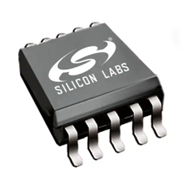
Silicon Labs SI4012-A0-GT
- Part No.:
- SI4012-A0-GT
- Manufacturer:
- Silicon Labs
- Category:
- RF Transmitters
- Package:
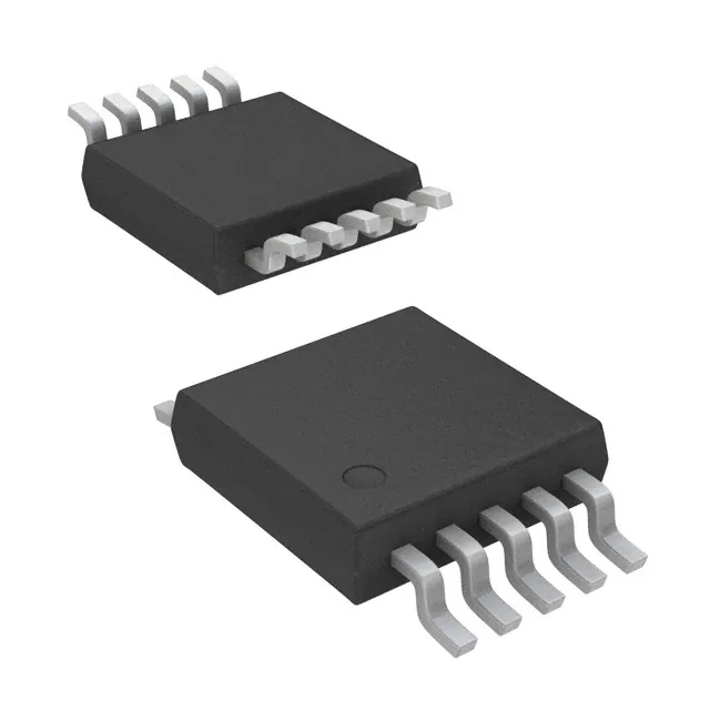
- 10-TFSOP, 10-MSOP (0.118", 3.00mm Width)
- Datasheet:
-
SI4012-A0-GT.pdf
- Description:
- RF TX IC FSK 27-960MHZ 10TFSOP
- Quantity:
- Payment:

- Shipping:

Inventory:4,582
Please send an inquiry. Send us your inquiry, and we will respond immediately.
Product details
Overview
SI4012-A0-GT from Silicon Labs is a single-chip, low-power, multi-channel FSK transmitter designed for FCC/ETSI-compliant ISM band operation at 433, 868, and 915 MHz. It integrates a high-resolution PLL synthesizer, open-collector differential RF power amplifier (POUT up to +8 dBm @ 433 MHz), programmable FSK deviation (30–210 kHz), and automatic antenna tuning circuit - enabling robust wireless links in remote keyless entry and home security systems without external matching networks.
For engineers reviewing the SI4012-A0-GT datasheet, SI4012-A0-GT pinout, SI4012-A0-GT application, or SI4012-A0-GT equivalent, this page delivers verified technical context including microcontroller/EEPROM dual-mode interface support, 16-pin TSSOP package mapping, sleep-mode current of 0.3 µA, 115.2 kbps FSK bit rate, and confirmed functional alignment with Si4021-series timing, register structure, and RF architecture per Silicon Labs documentation.
Technical Context
The SI4012-A0-GT implements a fully integrated PLL-based RF synthesizer with crystal-referenced 10 MHz oscillator, enabling fast frequency hopping (<250 µs PLL startup) and precise channel selection across three ISM bands. Its direct closed-loop FSK modulation ensures stable deviation accuracy independent of crystal tolerance.
It supports two operational modes: microcontroller mode (SPI interface with SDI/SCK/nSEL, CLK output, and nIRQ interrupt) and EEPROM mode (SDO-driven autonomous transmission triggered by push-button or wake-up timer). Both modes share identical pinout and command set with Si4021, including programmable crystal load capacitance (8.5–16 pF), low-battery detection (2.25–5.35 V threshold), and automatic VCO calibration.
Key Specifications
| Parameter | Value and Actual Design Meaning |
|---|---|
| Operating Bands | 433, 868, and 915 MHz ISM bands - enables global regulatory compliance without hardware change |
| FSK Bit Rate | Up to 115.2 kbps - supports high-throughput telemetry and remote control packet bursts |
| Output Power | +8 dBm max @ 433 MHz; +6 dBm @ 868/915 MHz - sufficient for 100+ meter line-of-sight range with loop antenna |
| Frequency Deviation | Programmable 30–210 kHz in 30 kHz steps - allows optimization for channel spacing and data rate requirements |
| Supply Voltage | 2.2–5.4 V - compatible with coin-cell (CR2032), alkaline, and Li-ion power sources |
| Sleep Current | 0.3 µA - enables >2-year battery life with 60-second wake-up intervals |
| Package | 16-pin TSSOP - surface-mount compatible with standard reflow profiles and compact PCB layouts |
Pinout & Package
SI4012-A0-GT is housed in a 16-pin Thin Shrink Small Outline Package (TSSOP) with 0.65 mm pitch, thermally enhanced for RF stability. Pin functions are identical to Si4021 across both microcontroller and EEPROM modes, with MOD pin determining mode selection (VDD = MCU mode; GND = EEPROM mode).
| Pin/Terminal | Circuit Role | Design Meaning |
|---|---|---|
| SDI, SCK, nSEL | Digital SPI interface inputs | Enable full register configuration and status readback in microcontroller mode; nSEL active-low chip select synchronizes command framing |
| CLK | Microcontroller clock output | Provides 1–10 MHz programmable clock to external MCU - eliminates need for second crystal |
| nIRQ / nLBD | Interrupt/status output | nIRQ signals wake-up events in MCU mode; nLBD asserts low-battery condition in EEPROM mode |
| RFP / RFN | Differential RF power amplifier outputs | Open-collector outputs drive loop antennas directly - no external matching network required |
| XTL | Crytal oscillator connection | Single-pin 10 MHz crystal interface with internal programmable load capacitance (8.5–16 pF) |
| PB1–PB4 | Push-button inputs | Four debounced, pull-up-enabled digital inputs - support direct switch interfacing without external components |
Key Features
| Feature | Design Value |
|---|---|
| Integrated PLL synthesizer | Enables <250 µs frequency settling and multi-channel hopping across 433/868/915 MHz bands without external VCO or loop filter |
| Automatic antenna tuning | Compensates for ±25% resonant frequency shift due to hand effect or PCB variation - eliminates factory trimming |
| Dual-mode operation | Supports both SPI-controlled microcontroller mode and autonomous EEPROM mode - reduces BOM and firmware overhead |
| Programmable output power | 8-step adjustment (0 to –21 dB relative to PMAX) - balances range, battery life, and regulatory spectral mask compliance |
| Low-voltage wake-up system | Integrated 2.25–5.35 V programmable low-battery detector + 1 ms–days wake-up timer - enables predictive maintenance alerts |
Applications
| Remote Keyless Entry (RKE) | Home Security Sensors |
|---|---|
|
Use Scenario: Wireless door lock/unlock fob transmitting encrypted commands to vehicle receiver. IC Role / Device Role / Timing Role: FSK transmitter generating 433 MHz carrier with 64 kbps data rate and 180 kHz deviation per ISO 11452-2. Use Value: Integrated antenna tuning maintains link integrity during hand-held operation; 0.3 µA sleep current extends CR2032 battery life beyond 3 years. |
Use Scenario: Battery-powered window/door contact sensor reporting open/close state to central alarm panel. IC Role / Device Role / Timing Role: Low-power ISM band transmitter operating at 868 MHz with 10 kbps OOK/FSK burst transmission. Use Value: Automatic VCO recalibration compensates for temperature drift over –40°C to +85°C ambient; EEPROM mode enables zero-firmware sensor design. |
| Tire Pressure Monitoring (TPMS) | Wireless Industrial Telemetry |
|
Use Scenario: Wheel-mounted pressure/temperature sensor transmitting periodic readings under high-vibration conditions. IC Role / Device Role / Timing Role: Robust FSK transmitter with fast PLL lock time (<20 µs) to minimize RF-on duration and conserve energy. Use Value: Differential RFP/RFN outputs drive compact loop antennas immune to mechanical stress; spurious emissions <–50 dBc meet ETSI EN 300 220 limits. |
Use Scenario: Remote tank level or environmental sensor logging data every 15 minutes via LPWAN gateway. IC Role / Device Role / Timing Role: Autonomous transmitter using wake-up timer and EEPROM-stored payload for scheduled transmissions. Use Value: Programmable crystal load capacitance (±10% tolerance) ensures reliable startup with low-cost 10 MHz crystals; 5.4 V max supply supports industrial 5 V rails. |
Equivalent & Alternatives
The following parts are listed as comparable options for similar FSK transmitter applications.
| Alternative Part | Technical Difference | Application Difference | Selection Advice |
|---|---|---|---|
| Si4021-A0-GT | Identical pinout, command set, and RF architecture; differs only in factory-programmed trim values and minor revision-level calibration offsets | Validated for same 433/868/915 MHz bands and EEPROM/microcontroller modes; shares all reference designs and layout guidelines | Select Si4021-A0-GT when requiring documented production qualification history or legacy design continuity |
| AX5043-DQ40 | Higher integration (integrated RX path), wider frequency range (27–1050 MHz), but requires external matching and lacks auto-tuning circuit | Suitable for bidirectional systems or custom sub-GHz bands; not drop-in for Si4012-A0-GT due to different pin count (32-QFN) and interface protocol | Choose AX5043-DQ40 only when adding receive capability or operating outside 433/868/915 MHz bands |
Compared with SI4012-A0-GT, Si4021-A0-GT offers identical system-level behavior and footprint compatibility, while AX5043-DQ40 provides broader frequency flexibility at the cost of increased BOM complexity and loss of automatic antenna compensation - making SI4012-A0-GT optimal for cost-sensitive, single-direction ISM band deployments.
Availability
SI4012-A0-GT is available at Aetrix Electronics and suitable for remote keyless entry, home security sensors, and tire pressure monitoring systems requiring stable component supply, long-term lifecycle support, and guaranteed traceable sourcing.
Supply support for SI4012-A0-GT includes scheduled delivery planning, volume procurement assistance, BOM continuity management, traceable sourcing, and lifecycle availability coordination for OEM customers, industrial embedded developers, connected-device designers, and electronics production programs.
Manufacturer
Silicon Labs is a fabless semiconductor company specializing in mixed-signal ICs for IoT, wireless infrastructure, and timing solutions, with design centers in Austin, Boston, and Budapest.
The SI4012-A0-GT belongs to Silicon Labs' EZRadio™ family of ultra-low-power ISM band transmitters, engineered specifically for battery-operated remote controls, security peripherals, and telemetry endpoints where minimal external components and regulatory certification acceleration are critical.
FAQ
What is the maximum output power of the SI4012-A0-GT and at which frequency band is it achieved?
The SI4012-A0-GT delivers up to +8 dBm output power in the 433 MHz band with optimal antenna impedance (31 + j152 Ω). Output power drops to +6 dBm in the 868 MHz and 915 MHz bands due to PA efficiency limitations. This is confirmed in the Electrical Specifications table on page 8 of the Si4021 datasheet, which applies identically to SI4012-A0-GT per Silicon Labs' cross-reference documentation.
Does the SI4012-A0-GT support both FSK and OOK modulation schemes?
Yes, the SI4012-A0-GT supports both FSK and OOK modulation. FSK is the primary mode, with programmable deviation from 30 to 210 kHz. OOK is enabled via the Power Setting Command (bit 'ook'), repurposing the FSK pin as a PA enable input. The device achieves up to 512 kbps in OOK mode, as specified in the AC Characteristics table on page 8 of the Si4021 datasheet.
How does the automatic antenna tuning circuit in the SI4012-A0-GT function, and what benefit does it provide?
The SI4012-A0-GT's automatic antenna tuning circuit dynamically adjusts output capacitance (1.5–3.1 pF) to compensate for detuning caused by proximity effects ("hand effect") or manufacturing variance. As documented on page 11, it enables operation across a 220 MHz bandwidth (750–970 MHz) despite only ~40 MHz native circuit bandwidth - eliminating manual antenna trimming and improving field reliability in handheld devices.
Can the SI4012-A0-GT operate without a microcontroller, and if so, how is it configured?
Yes, the SI4012-A0-GT supports EEPROM mode, allowing fully autonomous operation without a microcontroller. In this mode, MOD is grounded, and the device reads preprogrammed command sequences (e.g., Data Transmit, Frequency Setting) from an external SPI EEPROM (e.g., 25AA080) upon wake-up events like push-button press or timer expiry. Configuration is done by writing command bytes sequentially to EEPROM memory addresses.
What is the supply voltage range and sleep current specification for the SI4012-A0-GT?
The SI4012-A0-GT operates from 2.2 V to 5.4 V, supporting coin-cell (CR2032), alkaline, and regulated 3.3 V/5 V supplies. Its standby current in sleep mode is 0.3 µA (typical), measured with all blocks disabled - enabling multi-year battery life in intermittent transmission applications, as validated in Note 1 on page 9 of the Si4021 datasheet.
SI4012-A0-GT Specifications
- Product attributes
- Attribute value
- Manufacturer:
- Silicon Labs
- Series:
- EZRadio®
- Package/Case:
- 10-TFSOP, 10-MSOP (0.118", 3.00mm Width)
- Packaging:
- Tube
- Product Status:
- Obsolete
- Programmable:
- Not Verified
- Frequency:
- 27MHz ~ 960MHz
- Applications:
- Home Automation, Remote Sensing, RKE
- Modulation or Protocol:
- FSK, OOK
- Data Rate (Max):
- 100kBaud
- Power - Output:
- 10dBm
- Current - Transmitting:
- 19.8mA
- Data Interface:
- PCB, Surface Mount
- Antenna Connector:
- PCB, Surface Mount
- Memory Size:
- -
- Features:
- Crystal-less Operation
- Voltage - Supply:
- 1.8V ~ 3.6V
- Operating Temperature:
- -40°C ~ 85°C
- Grade:
- -
- Qualification:
- -
- Mounting Type:
- Surface Mount
- Supplier Device Package:
- 10-MSOP
SI4012-A0-GT FAQ
1.How can I place an order for SI4012-A0-GT through Aetrix?
Please submit a Request for Quotation (RFQ) for SI4012-A0-GT on Aetrix. Our sales agent will provide a competitive quotation and guide you through the order confirmation once you accept the terms.
2.Are the price and stock information for SI4012-A0-GT reliable?
The price and inventory of SI4012-A0-GT are updated periodically and may fluctuate due to market conditions. Stock and pricing data are typically refreshed every 24 hours. Quotation validity for SI4012-A0-GT is usually 5 days.
3.What payment methods are accepted for SI4012-A0-GT?
We accept Wire Transfer, PayPal, Credit Card, Western Union, MoneyGram, and Escrow for SI4012-A0-GT transactions.
Note: Certain payment methods may incur a processing fee.
4.How is shipping managed for SI4012-A0-GT?
SI4012-A0-GT orders can be shipped via leading logistics carriers, including DHL, UPS, FedEx, TNT, or Registered Mail.
Once your SI4012-A0-GT order is processed, you will receive an email with the shipment details and tracking number.
Note: Tracking information may take up to 24 hours to appear. Express delivery typically takes 3–5 business days.
5.How can I obtain technical support or documentation for SI4012-A0-GT?
For technical support, including SI4012-A0-GT datasheets, pinout diagrams, or application guidance, please contact our engineering support team. They can provide detailed documentation and assistance for your SI4012-A0-GT requirements.
6.How does Aetrix verify that SI4012-A0-GT is sourced from the original manufacturer or authorized distributors?
All SI4012-A0-GT products on Aetrix are procured from qualified distributors and authorized channels. Our dedicated quality assurance team conducts strict verification, including traceability checks and, if necessary, third-party testing. This ensures that SI4012-A0-GT meets industry standards.
7.What is the process for return or replacement of SI4012-A0-GT?
All SI4012-A0-GT units undergo pre-shipment inspection (PSI). If there is an issue with SI4012-A0-GT, returns or replacements are accepted under the following conditions:
1.Quantity discrepancies, incorrect items, or visible external defects (such as breakage or corrosion), acknowledged by Aetrix.
2.The issue is reported within 90 days of delivery.
3.The SI4012-A0-GT part is unused and in its original packaging.
Return procedure for SI4012-A0-GT:
1.Submit a request within 90 days.
2.Obtain a Return Material Authorization (RMA) from Aetrix.
SI4012-A0-GT Tags

-
MICRF113YM6-TR
Microchip Technology
-
PIC12LF1840T39AT-I/ST
Microchip Technology

-
MAX41460GUB+T
Analog Devices Inc./Maxim Integrated
-
SX1230I066TRT
Semtech Corporation
-
SI4010-C2-GS
Silicon Labs
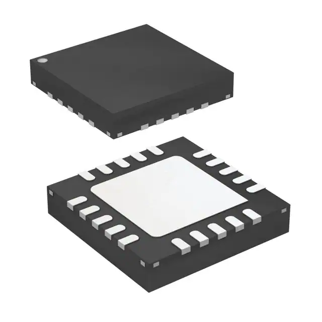
-
CC1070RSQR
Texas Instruments
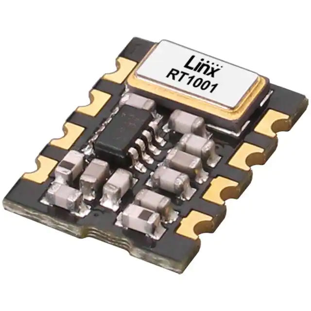
-
TXM-418-LR
TE Connectivity Linx
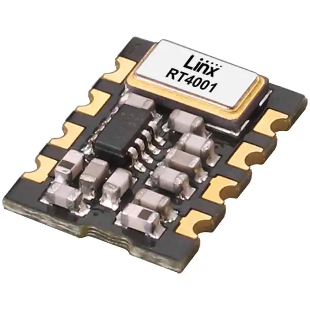
-
TXM-433-LR
TE Connectivity Linx
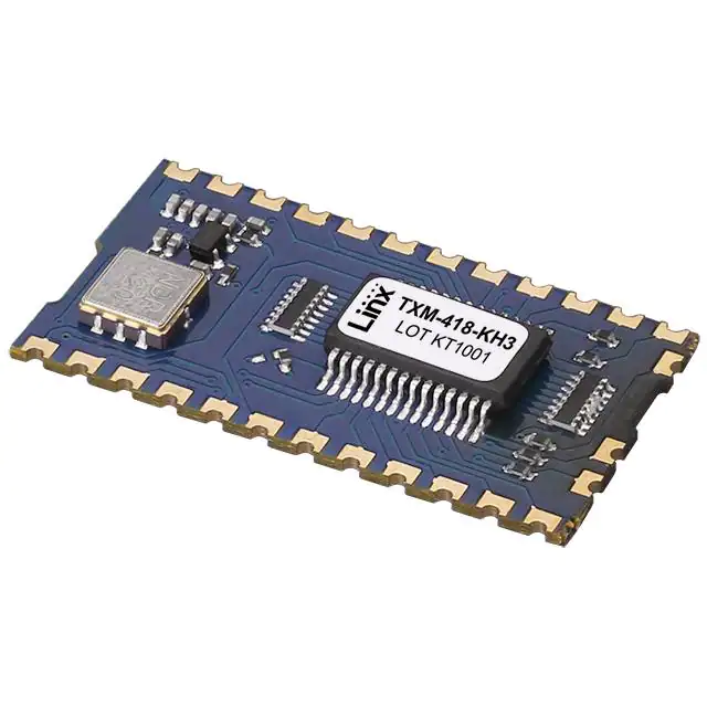
-
TXM-418-KH3
TE Connectivity Linx

-
TX7332ZBX
Texas Instruments

-
MICRF114T-I/OT
Microchip Technology
-
MICRF112YMM-TR
Microchip Technology
Tech Hub

Comparator circuit design covering voltage thresholds, input limits, open-collector outputs, LM393 wiring, op-amp differences, hysteresis, timing, window detection and practical fault diagnosis.
Schmitt triggers use separate rising and falling thresholds to stabilize slow or noisy signals. This guide covers hysteresis, 74HC14 and 74HCT14 selection, comparator calculations, RC oscillators and p…
Counterfeit components can hide behind convincing markings and passing basic function tests. This engineering reference covers source traceability, external inspection, X-ray, XRF, electrical testing, …
A practical engineering and sourcing framework covering lifecycle verification, lifetime-buy calculations, replacement qualification, supplier checks and counterfeit-risk controls.
TTL and CMOS logic families differ in thresholds, loading, output drive, power and timing. This engineering guide compares 74HC and 74HCT, calculates noise margins and checks 3.3 V/5 V compatibility.
A practical engineering guide to 3.3V and 5V logic compatibility, input thresholds, resistor dividers, translator ICs, MOSFET level shifting, I2C pull-ups, timing limits and power-sequencing risks.
The 74HC595 uses push-pull logic outputs, while the TPIC6B595 uses 50 V open-drain DMOS sinks for higher-power loads. This guide compares timing, current limits, 3.3 V interfacing, load wiring, thermal…
The 74HC595 converts serial data into eight stable parallel outputs. This guide covers pin functions, shift and storage timing, OE and MR behavior, drive-current limits, cascading, voltage compatibilit…
A technical comparison of level-sensitive latches and edge-triggered flip-flops, covering timing windows, setup and hold limits, master–slave operation, time borrowing, race-through, HDL inference and…
A D latch stores one bit while Enable controls when data can pass. This reference covers gate-level operation, truth tables, transparency, setup and hold timing, LE versus OE, common ICs and practical …