Vishay Siliconix SI9122EDLP-T1-E3
- Part No.:
- SI9122EDLP-T1-E3
- Manufacturer:
- Vishay Siliconix
- Category:
- DC DC Switching Controllers
- Package:
- PowerPAK® MLP65-20
- Datasheet:
-
SI9122EDLP-T1-E3.pdf
- Description:
- IC REG CTRLR HALF-BRG MLP65-20
- Quantity:
- Payment:

- Shipping:

Inventory:3,960
Please send an inquiry. Send us your inquiry, and we will respond immediately.
Product details
Overview
SI9122EDLP-T1-E3 from Vishay Siliconix is a 500-kHz half-bridge DC/DC controller IC with integrated secondary synchronous rectification drivers, designed for fixed telecom power systems (36–75 V input) delivering <3.3 V outputs. It provides ±1 A primary high-/low-side gate drive, programmable dead-time control via BBM pin, voltage-mode PWM with feedforward, and 135 °C overtemperature protection. It enables >90% efficiency in intermediate bus converters using synchronous rectification.
For engineers reviewing the SI9122EDLP-T1-E3 datasheet, SI9122EDLP-T1-E3 pinout, SI9122EDLP-T1-E3 application, or SI9122EDLP-T1-E3 equivalent, key selection criteria include its 20-pin MLP65-20 package, 36–75 V input range, 3.3 V reference output, dual current-sense inputs (CS1/CS2), and support for transformer-coupled SRH/SRL drive signals in isolated half-bridge topologies.
Technical Context
The SI9122EDLP-T1-E3 implements voltage-mode control with feedforward compensation and integrates a high-voltage pre-regulator (36–75 V input) to charge VCC during startup. Its internal oscillator sets nominal switching frequency at 500 kHz (adjustable 200–500 kHz via ROSC), and it features dedicated Break-Before-Make timing circuitry programmed by an external resistor on BBM pin.
It supports dual-loop operation: voltage loop via EP pin (inverting error amplifier input) and current loop via differential sense across CS1/CS2, enabling constant-current foldback and hiccup-free short-circuit protection. Secondary synchronous rectifier timing is transformer-isolated and sequenced independently from primary DH/DL outputs to prevent shoot-through.
Key Specifications
| Parameter | Value and Actual Design Meaning |
|---|---|
| Input Voltage Range | 36 V to 75 V - operates directly from telecom -48 V bus with margin; supports ETSI 300 132-2 compliance. |
| Oscillator Frequency | 200 kHz to 500 kHz - set by external ROSC resistor; 500 kHz nominal enables compact magnetics and high power density. |
| Reference Voltage | 3.3 V ±30 mV - stable bandgap reference for feedback loop; requires 0.1 µF external decoupling. |
| Primary Driver Output | ±1 A peak - drives high-/low-side MOSFETs directly; DH uses bootstrap (BST/LX), DL referenced to PGND. |
| Current Sense Inputs | CS1 and CS2 - differential pair with ±150 mV common-mode range; senses low-side primary switch current for OCP. |
| Overtemperature Protection | 135 °C activation - thermal shutdown with 22 °C hysteresis (OTP_off = 113 °C); improves reliability in industrial ambient. |
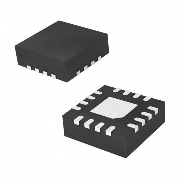
| Package | MLP65-20 - thermally enhanced 5 mm × 6 mm leadless package; θJA = 38 °C/W, suitable for high-power density layouts. |
Pinout & Package
SI9122EDLP-T1-E3 is housed in a 20-pin MLP65-20 (5 mm × 6 mm, 0.5 mm pitch) thermally enhanced leadless package with exposed pad (EP) for improved heat dissipation. The package is RoHS-compliant and rated for -40 °C to +85 °C junction temperature.
| Pin/Terminal | Circuit Role | Design Meaning |
|---|---|---|
| VIN | High-voltage start-up supply input | Connects to telecom bus (36–75 V); powers internal pre-regulator during startup before VCC is established. |
| REG_COMP | External PNP pass transistor compensation | Stabilizes high-voltage pre-regulator loop when using external PNP; prevents oscillation during fault recovery. |
| VCC | Internal logic and driver supply | 10.5–13.2 V operating range; UVLO at 8.8 V; clamped at 14.5 V to protect internal circuitry. |
| VREF | 3.3 V precision reference output | Provides stable feedback reference; 50 mA sink capability; disabled in shutdown mode. |
| GND | Analog ground reference | Signal return for reference, error amplifier, and sensing circuits; separate from PGND. |
| ROSC | Oscillator frequency programming | Resistor-to-ground sets fOSC from 200–500 kHz; 30 kΩ yields ~500 kHz. |
| EP | Error amplifier inverting input | Receives opto-coupled feedback signal; 0 V = max duty cycle, 2 V = min duty cycle (inverted relationship). |
| VINDET | VIN under-voltage detection & feedforward | Resistive divider input; triggers shutdown below 350–720 mV; also supplies voltage feedforward signal. |
| CS1 / CS2 | Differential current sense inputs | Monitor voltage drop across low-side primary sense resistor; threshold: 100 mV (lower limit), 150 mV (upper limit). |
| CL_CONT | Current limit compensation node | Capacitor-connected node controlling duty cycle reduction and frequency foldback during overload. |
| BBM | Break-Before-Make delay programming | External resistor sets non-overlap time between primary and secondary drivers to prevent transformer shorting. |
| SS | Soft-start capacitor connection | 20 µA internal current source charges external capacitor; linear ramp from DMIN to DMAX over soft-start period. |
| SRL / SRH | Secondary synchronous rectifier drive outputs | Transformer-coupled gate drive signals for low-/high-side secondary MOSFETs; sequenced to avoid shoot-through. |
| PGND | Power ground return | Low-impedance return path for DH, DL, and LX currents; must be connected to exposed pad (EP) for thermal performance. |
| DL | Primary low-side gate driver output | Drives N-channel MOSFET source to PGND; 1 A sink/source; rise/fall time ≤35 ns with 3 nF load. |
| LX | Half-bridge switch node | Connects to high-side MOSFET source and transformer primary; used as bootstrap return for DH driver. |
| DH | Primary high-side gate driver output | Bootstrap-driven (BST–LX); 1 A sink/source; VOH = VBST – 0.3 V, VOL = VLX + 0.3 V. |
| BST | Bootstrap supply for DH driver | Charged via external diode/capacitor from LX during DL on-time; supports up to 113.2 V transient. |
Key Features
| Feature | Design Value |
|---|---|
| Integrated ±1 A primary drivers | Eliminates need for external gate driver ICs; supports direct drive of high-current MOSFETs in half-bridge topology. |
| Programmable Break-Before-Make (BBM) | Prevents simultaneous conduction of primary and secondary switches via external RBBM; avoids transformer shorting and loss spikes. |
| Voltage feedforward compensation | Uses VINDET signal to dynamically adjust duty cycle vs. input variation; improves line regulation and transient response. |
| Frequency foldback under overload | Reduces switching frequency to ~100 kHz during severe overcurrent; maintains constant current without excessive MOSFET stress. |
| Advanced current limiting with hysteresis | Detects overcurrent via CS1/CS2; initiates controlled duty reduction then foldback, avoiding current tails and enabling fast recovery. |
| High-voltage pre-regulator with soft-start | Starts up from 36 V bus without auxiliary supply; internal 40 mA current-limited pre-regulator charges VCC before enabling PWM. |
Applications
| Intermediate Bus Converter | Brick Converter Module |
|---|---|
|
Use Scenario: 48 V input stepped down to 3.3 V or 5 V for point-of-load regulation in telecom shelf systems. IC Role / Device Role / Timing Role: Half-bridge controller managing primary switching and synchronizing secondary rectifiers via SRH/SRL outputs. Use Value: Achieves >92% efficiency at low output voltages by replacing Schottky diodes with synchronous MOSFETs driven by SI9122EDLP-T1-E3. |
Use Scenario: Compact, isolated 200–500 W DC/DC module for datacom equipment requiring high power density. IC Role / Device Role / Timing Role: Core timing and drive controller for half-bridge power stage; coordinates primary DH/DL and secondary SRH/SRL with BBM timing. Use Value: Enables use of smaller magnetics and capacitors via 500 kHz operation while maintaining robust OCP and thermal protection. |
| Distributed Power System | Network Card Power Supply |
|
Use Scenario: Local 12 V or 5 V generation from 48 V backplane in modular router or switch line cards. IC Role / Device Role / Timing Role: Isolated half-bridge controller with opto-coupled feedback (via EP pin) and transformer-driven synchronous rectification. Use Value: Delivers stable, low-noise output with fast transient response due to voltage-mode control and feedforward compensation. |
Use Scenario: On-board 3.3 V supply for FPGA, ASIC, or PHY interfaces on high-speed network interface cards. IC Role / Device Role / Timing Role: Fixed-frequency PWM controller with integrated current sensing and soft-start for reliable cold-boot behavior. Use Value: Prevents inrush current damage during hot-plug events via programmable soft-start and constant-current startup into large capacitive loads. |
Equivalent & Alternatives
The following parts are listed as comparable options for similar half-bridge controller applications.
| Alternative Part | Technical Difference | Application Difference | Selection Advice |
|---|---|---|---|
| UCC2895DW | 4-phase interleaved controller with adaptive dead-time; no integrated secondary SR drivers; requires external gate drivers for SR. | Targeted at higher-power (>500 W), multi-phase designs; lacks transformer-isolated SRH/SRL outputs. | Choose UCC2895DW only if scaling beyond single half-bridge or needing phase interleaving; SI9122EDLP-T1-E3 offers simpler SR integration. |
| LT3748IMS | Isolated flyback controller with integrated MOSFET drivers; no half-bridge topology support; operates up to 1 MHz. | Designed for non-isolated or flyback-based solutions; not pin- or functionally compatible with half-bridge synchronous rectification. | Use LT3748IMS for flyback-derived isolated supplies; SI9122EDLP-T1-E3 remains preferred for fixed telecom half-bridge with secondary sync rectification. |
Compared with UCC2895DW and LT3748IMS, SI9122EDLP-T1-E3 uniquely integrates transformer-coupled SRH/SRL outputs and BBM timing for half-bridge synchronous rectification-enabling >90% efficiency at sub-3.3 V outputs without external SR drivers or complex timing coordination.
Availability
SI9122EDLP-T1-E3 is available at Aetrix Electronics and suitable for intermediate bus converters, brick modules, distributed power systems, and network card power supplies requiring stable component supply and long-term industrial availability.
Supply support for SI9122EDLP-T1-E3 includes scheduled delivery planning, volume procurement assistance, BOM continuity management, traceable sourcing, and lifecycle availability coordination for OEM customers, industrial embedded developers, connected-device designers, and electronics production programs.
Manufacturer
Vishay Siliconix is a global leader in discrete semiconductors and passive components, specializing in high-reliability power MOSFETs, diodes, and analog ICs for industrial, telecom, and automotive markets.
The Si9122E product line was engineered specifically for high-efficiency, isolated half-bridge DC/DC conversion in fixed telecom infrastructure, emphasizing robust startup, synchronous rectification control, and thermal resilience in compact packages like MLP65-20.
FAQ
What is the recommended minimum external ROSC resistor value for SI9122EDLP-T1-E3?
The SI9122EDLP-T1-E3 datasheet specifies ROSC values from 30 kΩ to 72 kΩ for 200–500 kHz operation. A 30 kΩ resistor yields ~500 kHz nominal frequency. Using less than 30 kΩ risks exceeding maximum oscillator frequency limits and may cause timing violations in BBM and driver sequencing. Always verify actual frequency with oscilloscope measurement under load conditions for SI9122EDLP-T1-E3.
How does SI9122EDLP-T1-E3 handle overcurrent protection during startup?
SI9122EDLP-T1-E3 employs advanced current limiting that activates immediately upon detecting VCS2–VCS1 >100 mV. During startup, it first reduces duty cycle toward DMIN; if current persists, it initiates frequency foldback to ~100 kHz. This prevents current tails and ensures safe charging of large output capacitors without triggering full shutdown-critical for reliable SI9122EDLP-T1-E3 operation in telecom modules.
Can SI9122EDLP-T1-E3 drive secondary MOSFETs without a pulse transformer?
No. SI9122EDLP-T1-E3's SRH and SRL outputs are designed exclusively for transformer-coupled drive to achieve galvanic isolation between primary and secondary sides. The outputs deliver complementary logic-level signals intended to drive center-tapped pulse transformers feeding inverter pairs. Direct MOSFET gate drive is not supported, and attempting it would violate isolation requirements and timing safety margins of SI9122EDLP-T1-E3.
What is the purpose of the REG_COMP pin on SI9122EDLP-T1-E3?
The REG_COMP pin on SI9122EDLP-T1-E3 provides frequency compensation for the external high-voltage pre-regulator when using a PNP pass transistor. It stabilizes the loop during transient events (e.g., startup or fault recovery) and prevents oscillation. Connecting an appropriate capacitor (typically 100–470 pF) between REG_COMP and GND ensures stable VCC regulation without slowing fault response-essential for robust SI9122EDLP-T1-E3 operation in telecom systems.
Does SI9122EDLP-T1-E3 support both voltage-mode and current-mode control simultaneously?
SI9122EDLP-T1-E3 operates primarily in voltage-mode control under normal conditions, using EP as the error amplifier input. However, it seamlessly transitions to current-mode behavior during overcurrent events via the CS1/CS2 sense path-triggering duty-cycle reduction and frequency foldback. This hybrid approach ensures stable regulation during steady state and fast, predictable protection during faults, making SI9122EDLP-T1-E3 suitable for demanding telecom power applications.
SI9122EDLP-T1-E3 Specifications
- Product attributes
- Attribute value
- Manufacturer:
- Vishay Siliconix
- Series:
- -
- Package/Case:
- PowerPAK® MLP65-20
- Packaging:
- Tape & Reel (TR)
- Product Status:
- Active
- Output Type:
- Transistor Driver
- Function:
- Step-Up/Step-Down
- Output Configuration:
- Positive, Isolation Capable
- Topology:
- Half-Bridge
- Number of Outputs:
- 1
- Output Phases:
- 1
- Voltage - Supply (Vcc/Vdd):
- 10.5V ~ 13.2V
- Frequency - Switching:
- 500kHz
- Duty Cycle (Max):
- 91%
- Synchronous Rectifier:
- Yes
- Clock Sync:
- No
- Serial Interfaces:
- -
- Control Features:
- Current Limit, Sequencing, Soft Start
- Operating Temperature:
- -40°C ~ 85°C (TA)
- Grade:
- -
- Qualification:
- -
- Mounting Type:
- Surface Mount
- Supplier Device Package:
- PowerPAK® MLP65-20
SI9122EDLP-T1-E3 FAQ
1.How can I place an order for SI9122EDLP-T1-E3 through Aetrix?
Please submit a Request for Quotation (RFQ) for SI9122EDLP-T1-E3 on Aetrix. Our sales agent will provide a competitive quotation and guide you through the order confirmation once you accept the terms.
2.Are the price and stock information for SI9122EDLP-T1-E3 reliable?
The price and inventory of SI9122EDLP-T1-E3 are updated periodically and may fluctuate due to market conditions. Stock and pricing data are typically refreshed every 24 hours. Quotation validity for SI9122EDLP-T1-E3 is usually 5 days.
3.What payment methods are accepted for SI9122EDLP-T1-E3?
We accept Wire Transfer, PayPal, Credit Card, Western Union, MoneyGram, and Escrow for SI9122EDLP-T1-E3 transactions.
Note: Certain payment methods may incur a processing fee.
4.How is shipping managed for SI9122EDLP-T1-E3?
SI9122EDLP-T1-E3 orders can be shipped via leading logistics carriers, including DHL, UPS, FedEx, TNT, or Registered Mail.
Once your SI9122EDLP-T1-E3 order is processed, you will receive an email with the shipment details and tracking number.
Note: Tracking information may take up to 24 hours to appear. Express delivery typically takes 3–5 business days.
5.How can I obtain technical support or documentation for SI9122EDLP-T1-E3?
For technical support, including SI9122EDLP-T1-E3 datasheets, pinout diagrams, or application guidance, please contact our engineering support team. They can provide detailed documentation and assistance for your SI9122EDLP-T1-E3 requirements.
6.How does Aetrix verify that SI9122EDLP-T1-E3 is sourced from the original manufacturer or authorized distributors?
All SI9122EDLP-T1-E3 products on Aetrix are procured from qualified distributors and authorized channels. Our dedicated quality assurance team conducts strict verification, including traceability checks and, if necessary, third-party testing. This ensures that SI9122EDLP-T1-E3 meets industry standards.
7.What is the process for return or replacement of SI9122EDLP-T1-E3?
All SI9122EDLP-T1-E3 units undergo pre-shipment inspection (PSI). If there is an issue with SI9122EDLP-T1-E3, returns or replacements are accepted under the following conditions:
1.Quantity discrepancies, incorrect items, or visible external defects (such as breakage or corrosion), acknowledged by Aetrix.
2.The issue is reported within 90 days of delivery.
3.The SI9122EDLP-T1-E3 part is unused and in its original packaging.
Return procedure for SI9122EDLP-T1-E3:
1.Submit a request within 90 days.
2.Obtain a Return Material Authorization (RMA) from Aetrix.
SI9122EDLP-T1-E3 Tags

-
UCC28C45DR
Texas Instruments

-
UCC28C40DR
Texas Instruments

-
UCC28C43DR
Texas Instruments

-
ZXSC410E6TA
Diodes Incorporated

-
LM3524DMX/NOPB
Texas Instruments

-
LM3489MMX/NOPB
Texas Instruments
-
MIC2102YML-TR
Microchip Technology

-
LM5148RGYR
Texas Instruments
-
TL598CDR
Texas Instruments

-
LM5155DSSR
Texas Instruments

-
LM25085MYX/NOPB
Texas Instruments

-
UCC2813DTR-0
Texas Instruments
Tech Hub

Comparator circuit design covering voltage thresholds, input limits, open-collector outputs, LM393 wiring, op-amp differences, hysteresis, timing, window detection and practical fault diagnosis.
Schmitt triggers use separate rising and falling thresholds to stabilize slow or noisy signals. This guide covers hysteresis, 74HC14 and 74HCT14 selection, comparator calculations, RC oscillators and p…
Counterfeit components can hide behind convincing markings and passing basic function tests. This engineering reference covers source traceability, external inspection, X-ray, XRF, electrical testing, …
A practical engineering and sourcing framework covering lifecycle verification, lifetime-buy calculations, replacement qualification, supplier checks and counterfeit-risk controls.
TTL and CMOS logic families differ in thresholds, loading, output drive, power and timing. This engineering guide compares 74HC and 74HCT, calculates noise margins and checks 3.3 V/5 V compatibility.
A practical engineering guide to 3.3V and 5V logic compatibility, input thresholds, resistor dividers, translator ICs, MOSFET level shifting, I2C pull-ups, timing limits and power-sequencing risks.
The 74HC595 uses push-pull logic outputs, while the TPIC6B595 uses 50 V open-drain DMOS sinks for higher-power loads. This guide compares timing, current limits, 3.3 V interfacing, load wiring, thermal…
The 74HC595 converts serial data into eight stable parallel outputs. This guide covers pin functions, shift and storage timing, OE and MR behavior, drive-current limits, cascading, voltage compatibilit…
A technical comparison of level-sensitive latches and edge-triggered flip-flops, covering timing windows, setup and hold limits, master–slave operation, time borrowing, race-through, HDL inference and…
A D latch stores one bit while Enable controls when data can pass. This reference covers gate-level operation, truth tables, transparency, setup and hold timing, LE versus OE, common ICs and practical …









