Send an Inquiry

To receive a quote for your project, please fill in the following information, and we’ll get back to you promptly.

Name*
Company*
Email Address*
Phone/WhatsApp
Part Number*
Quantity*
Message
Submit Inventory List

Please fill in the following information, and we’ll get back to you promptly.

Name*
Company*
Email Address*
Phone/WhatsApp
Upload My List
Message

Vishay Siliconix SI9183DT-30-T1-E3

Part No.:
SI9183DT-30-T1-E3
Manufacturer:
Vishay Siliconix
Category:
Voltage Regulators - Linear, Low Drop Out (LDO) Regulators
Package:
SOT-23-5 Thin, TSOT-23-5
Datasheet:
AetrixSI9183DT-30-T1-E3.pdf
Description:
IC REG LINEAR 3V 150MA TSOT23-5
Quantity:
Payment:
Payment
Shipping:
Shipping

Inventory:1,620

Please send an inquiry. Send us your inquiry, and we will respond immediately.

Part Number
Quantity*
Price
Name*
Company
Email*
Comments

Product details

Overview

SI9183DT-30-T1-E3 from Vishay Siliconix is a fixed-output 3.0-V, 150-mA CMOS low-dropout (LDO) voltage regulator in Thin SOT-23-5 package. It delivers 135-mV dropout at 150-mA load, supports 300-mA peak current, uses ceramic output capacitors, and features shutdown control and thermal/short-circuit protection. It is designed for battery-powered portable systems requiring stable, low-noise 3.0-V supply.

For engineers reviewing the SI9183DT-30-T1-E3 datasheet, SI9183DT-30-T1-E3 pinout, SI9183DT-30-T1-E3 application, or SI9183DT-30-T1-E3 equivalent, key selection criteria include guaranteed 3.0-V ±2.5% accuracy across −40°C to +85°C, 100-μVrms output noise with 0.1-μF CBP capacitor, fast 30-mV load transient response, and 1-μA shutdown current - all critical for power-sensitive embedded designs.

Technical Context

The SI9183DT-30-T1-E3 implements a CMOS-based LDO architecture with internal 1.215-V reference and error amplifier, enabling ultra-low ground current (500 μA typical at 150 mA) and high PSRR (60 dB at 1 kHz). Its bandwidth exceeds 50 kHz, supporting rapid line/load transients without external compensation.

It integrates a 6-MΩ internal pull-down on the SD pin, defines ON/OFF thresholds at VIH ≥ 1.2 V and VIL ≤ 0.4 V, and maintains stability with 1–10 μF ceramic output capacitors (X5R/X7R), eliminating need for tantalum or electrolytic types.

Key Specifications

ParameterValue and Actual Design Meaning
Output VoltageFixed 3.0 V ±2.5% over −40°C to +85°C - ensures reliable logic-level supply for 3.3-V I/O systems operating down to 3.0 V.
Dropout Voltage135 mV at 150 mA - enables operation down to VIN = 3.135 V, maximizing usable battery voltage range in single-cell Li-ion or dual-cell alkaline systems.
Ground Current500 μA typical at 150 mA - minimizes quiescent power loss, extending standby time in always-on portable devices.
Output Noise100 μVrms (50 Hz–100 kHz) with 0.1-μF CBP capacitor - meets low-noise requirements for RF front-ends and precision analog circuitry.
Shutdown Current1 μA maximum - reduces system leakage during sleep modes, critical for multi-year battery life in IoT sensors.
PSRR60 dB at 1 kHz - suppresses switching noise from upstream DC-DC converters, simplifying power domain isolation.
Thermal Shutdown165°C junction temperature with 20°C hysteresis - provides robust overtemperature protection without nuisance tripping during transient loads.

Pinout & Package

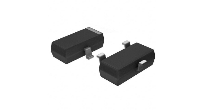
SI9183DT-30-T1-E3 is housed in a lead (Pb)-free Thin SOT-23-5 package (1.6 mm × 2.9 mm × 1.1 mm), optimized for space-constrained portable PCBs.

Pin/TerminalCircuit RoleDesign Meaning
1 - VINInput supplyAccepts 2–6 V input; requires ≥1-μF ceramic bypass to GND for stability and EMI suppression.
2 - GNDPower groundCommon return for VIN, VOUT, SD, and BP; must be low-impedance local ground plane connection.
3 - SDShutdown controlActive-high logic input; <0.4 V disables regulator (≤1 μA IIN(off)); ≥1.2 V enables regulation.
4 - BPNoise bypassConnects to 0.1-μF ceramic capacitor to GND to reduce internal reference noise and improve PSRR.
5 - VOUTRegulated outputDelivers 3.0 V ±2.5%; stable with 1–10 μF X5R/X7R ceramic capacitor to GND (ESR 0.4–4 Ω).

Key Features

FeatureDesign Value
Ultra-low dropout135 mV @ 150 mA enables >95% battery energy utilization in 3.0-V systems powered by 3.6-V Li-ion cells.
Fast transient response30-mV load step deviation (1→150 mA) with 2.2-μF COUT - maintains system stability during processor wake-up bursts.
Low-noise design100 μVrms noise with CBP capacitor supports clean power for ADCs, PLLs, and RF ICs without external filtering.
Integrated protectionThermal shutdown (165°C) and short-circuit limiting (400 mA) eliminate need for external fault management circuitry.
Ceramic-capacitor compatibleStable with 1–10 μF X5R/X7R ceramics - reduces BOM cost, size, and aging drift vs. tantalum alternatives.

Applications

Cellular Phone BasebandPDA Core Logic Supply

Use Scenario: Powering baseband processor core and memory interfaces in GSM/UMTS handsets with tight battery voltage swing (3.4–4.2 V).

IC Role / Device Role / Timing Role: Primary 3.0-V LDO delivering regulated supply with fast load transient response to handle burst-mode RF transmission.

Use Value: 135-mV dropout extends talk time by >12 minutes per charge cycle compared to bipolar LDOs; 100-μVrms noise prevents digital interference in sensitive RF receive paths.

Use Scenario: Providing clean 3.0-V rail to ARM9 application processor and NAND flash in handheld PDAs with intermittent high-current display backlighting.

IC Role / Device Role / Timing Role: Post-regulator for buck converter output, decoupling switching noise while maintaining tight voltage tolerance during backlight PWM transitions.

Use Value: 60-dB PSRR at 1 kHz attenuates buck converter ripple; shutdown mode draws only 1 μA, enabling multi-week standby without battery drain.

Notebook Computer USB PeripheralsWireless Sensor Node MCU Supply

Use Scenario: Powering USB 2.0 PHY and hub controller in ultraportable notebooks where 3.3-V rail is derived from higher-voltage battery bus.

IC Role / Device Role / Timing Role: Low-noise, fixed 3.0-V LDO ensuring USB signal integrity and meeting USB-IF VOH/VOL margins under dynamic load.

Use Value: 30-mV load transient deviation prevents USB packet corruption during enumeration; Thin SOT-23-5 footprint saves board area near USB connectors.

Use Scenario: Supplying 3.0-V to sub-GHz RF transceiver and 32-bit MCU in battery-operated industrial sensor nodes deployed for 10+ years.

IC Role / Device Role / Timing Role: Primary system regulator with shutdown controlled by MCU GPIO to gate power during deep-sleep intervals.

Use Value: 1-μA shutdown current enables >10-year battery life with 2000-mAh coin cell; −40°C to +85°C rating ensures field reliability in uncontrolled environments.

Equivalent & Alternatives

The following parts are listed as comparable options for similar LDO regulator applications.

Alternative PartTechnical DifferenceApplication DifferenceSelection Advice
MCP1700T-3002E/TT300-mA rated, 170-mV dropout at 250 mA, 2.5-µA quiescent current, SOT-23-3 package (no SD pin)Lacks shutdown control and BP pin; lower max current but higher IQ; requires external enable circuitry for power gatingSelect when board space is extremely constrained and shutdown is managed externally; not suitable for noise-sensitive RF sections.
Torex XC6206P302MR-G150-mA rated, 200-mV dropout at 100 mA, 1-µA shutdown current, SOT-25 package with SD pin, no BP pinHigher dropout reduces usable battery range; no noise-bypass capability limits use in precision analog/RF circuitsChoose for cost-sensitive, non-noise-critical applications where 3.0-V accuracy and thermal protection are primary requirements.

Compared with MCP1700T-3002E/TT and XC6206P302MR-G, SI9183DT-30-T1-E3 uniquely combines ultra-low dropout (135 mV), integrated noise reduction (BP pin), and full protection set in a 5-pin SOT-23 - making it optimal for compact, battery-limited, noise-sensitive portable electronics where every millivolt and microamp matters.

Availability

SI9183DT-30-T1-E3 is available at Aetrix Electronics and suitable for cellular phones, PDAs, notebook peripherals, and wireless sensor nodes requiring stable component supply, long-term lifecycle support, and Pb-free compliance.

Supply support for SI9183DT-30-T1-E3 includes scheduled delivery planning, volume procurement assistance, BOM continuity management, traceable sourcing, and lifecycle availability coordination for OEM customers, industrial embedded developers, connected-device designers, and electronics production programs.

Manufacturer

Vishay Siliconix is a global semiconductor manufacturer specializing in discrete components and analog ICs, with leadership in power management, sensing, and passive technologies.

The Si9183 family was engineered specifically for battery-powered portable electronics, emphasizing ultra-low dropout, minimal quiescent current, and fast transient response to maximize runtime and signal integrity.

FAQ

What is the guaranteed output voltage tolerance of SI9183DT-30-T1-E3 over temperature?

The SI9183DT-30-T1-E3 guarantees ±2.5% output voltage accuracy across the full operating ambient temperature range of −40°C to +85°C, as specified in the datasheet's "Output Voltage Accuracy (Fixed Versions)" parameter. This tolerance applies under 1–150 mA load conditions and ensures reliable 3.0-V operation for logic interfaces even in extreme environmental conditions. The SI9183DT-30-T1-E3 achieves this via an internal trimmed 1.215-V bandgap reference and precision feedback network.

Does SI9183DT-30-T1-E3 require an external capacitor on the BP pin for basic operation?

No, the SI9183DT-30-T1-E3 operates fully functional without a capacitor on the BP pin. The BP (bypass) pin is optional and used only to reduce output noise - connecting a 0.1-μF ceramic capacitor from BP to GND lowers RMS noise from 300 μV to 100 μV (50 Hz–100 kHz). For non-noise-critical applications like digital logic rails, omitting the BP capacitor is acceptable and simplifies the BOM. The SI9183DT-30-T1-E3 remains stable and within spec regardless.

What is the minimum input voltage required for SI9183DT-30-T1-E3 to maintain regulation at 150 mA load?

The SI9183DT-30-T1-E3 requires a minimum input voltage of 3.135 V to maintain 3.0-V regulation at 150 mA load, based on its guaranteed 180-mV maximum dropout voltage over temperature (−40°C to +85°C). At room temperature, typical dropout is 135 mV, so VIN ≥ 3.135 V ensures regulation across full temp/load conditions. Input below 3.135 V causes VOUT to droop proportionally - the SI9183DT-30-T1-E3 does not regulate below this threshold.

Can SI9183DT-30-T1-E3 drive a 10-μF ceramic output capacitor?

Yes, the SI9183DT-30-T1-E3 is explicitly characterized and guaranteed stable with output capacitors ranging from 1 μF to 10 μF, including X5R and X7R ceramic types. The datasheet confirms stability across this full range under all load conditions (0–150 mA), eliminating need for external compensation. Using 10 μF improves load transient response and reduces output impedance at higher frequencies - a valid design choice for systems with dynamic current demands. The SI9183DT-30-T1-E3's internal compensation is optimized for this capacitor range.

How does the shutdown function of SI9183DT-30-T1-E3 behave when the SD pin is left floating?

When the SD pin of SI9183DT-30-T1-E3 is left floating, its internal 6-MΩ pull-down resistor pulls the pin to GND, forcing the device into shutdown mode with ≤1 μA supply current. This fail-safe behavior prevents unintended activation and conserves battery power. To enable regulation, SD must be actively driven to ≥1.2 V (e.g., tied to VIN or a GPIO). The SI9183DT-30-T1-E3 datasheet specifies VIH(min) = 1.2 V and VIL(max) = 0.4 V, confirming robust noise margin for reliable control.

SI9183DT-30-T1-E3 Specifications

Product attributes
Attribute value
Manufacturer:
Vishay Siliconix
Series:
-
Package/Case:
SOT-23-5 Thin, TSOT-23-5
Packaging:
Tape & Reel (TR)
Product Status:
Obsolete
Output Configuration:
Positive
Output Type:
Fixed
Number of Regulators:
1
Voltage - Input (Max):
6V
Voltage - Output (Min/Fixed):
3V
Voltage - Output (Max):
-
Voltage Dropout (Max):
0.22V @ 150mA
Current - Output:
150mA
Current - Quiescent (Iq):
900 µA
Current - Supply (Max):
-
PSRR:
60dB ~ 30dB (1kHz ~ 100kHz)
Control Features:
Enable
Protection Features:
Over Temperature, Short Circuit
Operating Temperature:
-40°C ~ 85°C
Grade:
-
Qualification:
-
Mounting Type:
Surface Mount
Supplier Device Package:
TSOT-23-5

SI9183DT-30-T1-E3 FAQ

1.How can I place an order for SI9183DT-30-T1-E3 through Aetrix?

Please submit a Request for Quotation (RFQ) for SI9183DT-30-T1-E3 on Aetrix. Our sales agent will provide a competitive quotation and guide you through the order confirmation once you accept the terms.

2.Are the price and stock information for SI9183DT-30-T1-E3 reliable?

The price and inventory of SI9183DT-30-T1-E3 are updated periodically and may fluctuate due to market conditions. Stock and pricing data are typically refreshed every 24 hours. Quotation validity for SI9183DT-30-T1-E3 is usually 5 days.

3.What payment methods are accepted for SI9183DT-30-T1-E3?

We accept Wire Transfer, PayPal, Credit Card, Western Union, MoneyGram, and Escrow for SI9183DT-30-T1-E3 transactions.

Note: Certain payment methods may incur a processing fee.

4.How is shipping managed for SI9183DT-30-T1-E3?

SI9183DT-30-T1-E3 orders can be shipped via leading logistics carriers, including DHL, UPS, FedEx, TNT, or Registered Mail.

Once your SI9183DT-30-T1-E3 order is processed, you will receive an email with the shipment details and tracking number.

Note: Tracking information may take up to 24 hours to appear. Express delivery typically takes 3–5 business days.

5.How can I obtain technical support or documentation for SI9183DT-30-T1-E3?

For technical support, including SI9183DT-30-T1-E3 datasheets, pinout diagrams, or application guidance, please contact our engineering support team. They can provide detailed documentation and assistance for your SI9183DT-30-T1-E3 requirements.

6.How does Aetrix verify that SI9183DT-30-T1-E3 is sourced from the original manufacturer or authorized distributors?

All SI9183DT-30-T1-E3 products on Aetrix are procured from qualified distributors and authorized channels. Our dedicated quality assurance team conducts strict verification, including traceability checks and, if necessary, third-party testing. This ensures that SI9183DT-30-T1-E3 meets industry standards.

7.What is the process for return or replacement of SI9183DT-30-T1-E3?

All SI9183DT-30-T1-E3 units undergo pre-shipment inspection (PSI). If there is an issue with SI9183DT-30-T1-E3, returns or replacements are accepted under the following conditions:

1.Quantity discrepancies, incorrect items, or visible external defects (such as breakage or corrosion), acknowledged by Aetrix.

2.The issue is reported within 90 days of delivery.

3.The SI9183DT-30-T1-E3 part is unused and in its original packaging.

Return procedure for SI9183DT-30-T1-E3:

1.Submit a request within 90 days.

2.Obtain a Return Material Authorization (RMA) from Aetrix.

SI9183DT-30-T1-E3 Tags

  • SI9183DT-30-T1-E3
  • SI9183DT-30-T1-E3 PDF
  • SI9183DT-30-T1-E3 Datasheet
  • SI9183DT-30-T1-E3 Specifications
  • SI9183DT-30-T1-E3 Images
  • Vishay Siliconix
  • Vishay Siliconix SI9183DT-30-T1-E3
  • Buy SI9183DT-30-T1-E3
  • SI9183DT-30-T1-E3 Price
  • SI9183DT-30-T1-E3 Distributor
  • SI9183DT-30-T1-E3 Supplier
  • SI9183DT-30-T1-E3 Wholesale
Related Products
MIC5504-1.8YM5-TR
MIC5504-1.8YM5-TR

Microchip Technology

MIC5504-3.3YM5-TR
MIC5504-3.3YM5-TR

Microchip Technology

MIC5365-3.0YC5-TR
MIC5365-3.0YC5-TR

Microchip Technology

MIC5365-1.8YC5-TR
MIC5365-1.8YC5-TR

Microchip Technology

MIC5365-2.5YC5-TR
MIC5365-2.5YC5-TR

Microchip Technology

MIC5365-3.3YC5-TR
MIC5365-3.3YC5-TR

Microchip Technology

MIC5365-3.3YD5-TR
MIC5365-3.3YD5-TR

Microchip Technology

MIC5317-3.3YM5-TR
MIC5317-3.3YM5-TR

Microchip Technology

TLV1117LV33DCYR
TLV1117LV33DCYR

Texas Instruments

MIC5317-3.3YMT-TZ
MIC5317-3.3YMT-TZ

Microchip Technology

MIC5528-3.3YMT-TR
MIC5528-3.3YMT-TR

Microchip Technology

TLV75801PDRVR
TLV75801PDRVR

Texas Instruments

Tech Hub
Search

Search

PRODUCT

PRODUCT

PHONE

PHONE

USER

USER