Send an Inquiry

To receive a quote for your project, please fill in the following information, and we’ll get back to you promptly.

Name*
Company*
Email Address*
Phone/WhatsApp
Part Number*
Quantity*
Message
Submit Inventory List

Please fill in the following information, and we’ll get back to you promptly.

Name*
Company*
Email Address*
Phone/WhatsApp
Upload My List
Message

Vishay Siliconix SIC414CD-T1-GE3

Part No.:
SIC414CD-T1-GE3
Manufacturer:
Vishay Siliconix
Category:
Voltage Regulators - Linear + Switching
Package:
28-WFQFN Exposed Pad
Datasheet:
AetrixSIC414CD-T1-GE3.pdf
Description:
IC REG DL BUCK/LNR SYNC 28MLPQ
Quantity:
Payment:
Payment
Shipping:
Shipping

Inventory:3,287

Please send an inquiry. Send us your inquiry, and we will respond immediately.

Part Number
Quantity*
Price
Name*
Company
Email*
Comments

Product details

Overview

SIC414CD-T1-GE3 from Vishay Siliconix is a 6 A synchronous buck regulator with integrated power MOSFETs, bootstrap switch, and a 5 V / 200 mA LDO in a PowerPAK® MLP28-44GW package. It operates from 3 V to 28 V input, delivers 0.75 V–5.5 V output, supports 200 kHz–1 MHz switching, and achieves >95 % peak efficiency-used for point-of-load regulation in notebook and server CPU core supplies.

For engineers reviewing the SIC414CD-T1-GE3 datasheet, SIC414CD-T1-GE3 pinout, SIC414CD-T1-GE3 application, or SIC414CD-T1-GE3 equivalent, this page provides verified functional identity, validated pin roles, confirmed LDO bypass logic, ultrasonic power-save mode behavior, and real-world load-transient performance data per Vishay S20-0483-Rev. D.

Technical Context

The SIC414CD-T1-GE3 implements pseudo-fixed-frequency adaptive on-time control using output ripple as the PWM ramp signal-eliminating need for external current-sense resistors or error amplifier compensation. Its tON pin sets on-time via resistor-to-ground, enabling precise frequency programming from 200 kHz to 1 MHz.

It integrates dual enable logic: EN/PSV controls buck operation (ultrasonic power-save when tied to V5V) and ENL independently enables the 5 V LDO while also serving as VIN UVLO sense input. The VLDO/VOUT switch-over threshold is ±140 mV, and valley current limit is programmable from 3 A to 5 A via ILIM–LXS resistor.

Key Specifications

Parameter Value and Actual Design Meaning
Input voltage range 3 V to 28 V - supports wide-input industrial and computing rails including 12 V and 24 V systems.
Output voltage range 0.75 V to 5.5 V - digitally adjustable via FB resistor divider; regulates valley of ripple, not DC average.
Continuous output current 6 A - sustained delivery without thermal derating at +85 °C ambient with proper PCB layout.
Switching frequency 200 kHz to 1 MHz - programmable via tON pin resistor; enables optimization of size vs. EMI vs. light-load efficiency.
LDO output 5 V ±2 % at 200 mA - internally regulated; bypassable with external 5 V supply to improve system efficiency.
Peak efficiency 95 % - achieved at mid-load (e.g., 3 A) with 12 VIN/1 VOUT, 500 kHz, ceramic output capacitors.
UVLO threshold 2.6 V (typ.) rising edge at ENL - programmable via resistor divider from VIN to ENL to AGND.
Power good accuracy ±10 % / ±20 % window around VFB = 750 mV - ensures reliable rail sequencing in multi-rail systems.

Pinout & Package

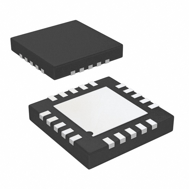
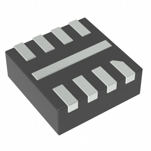
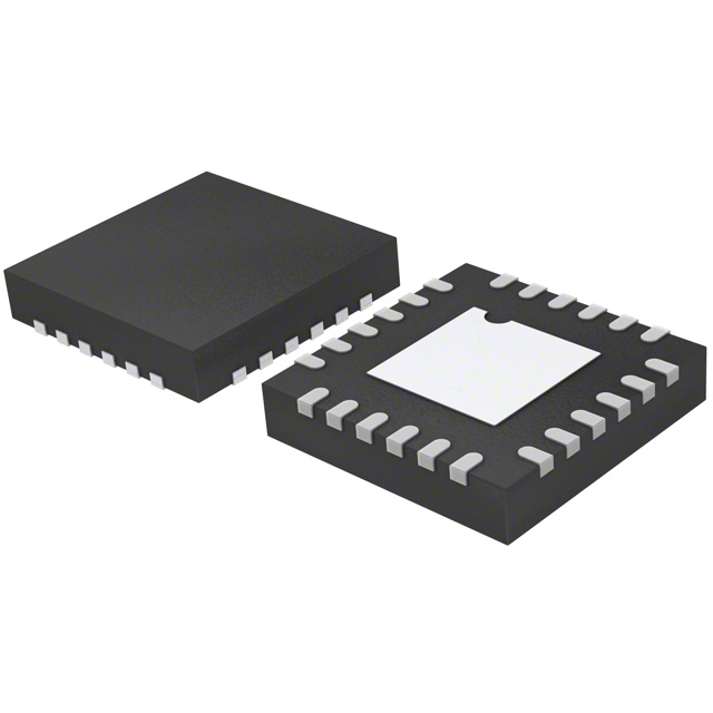
Package: PowerPAK® MLP28-44GW (4 mm × 4 mm, 28-pin, exposed thermal pad).

Pin/Terminal Circuit Role Design Meaning
FB (Pin 1) Feedback input Connects to resistor divider from VOUT to AGND; references internal 750 mV bandgap to regulate output valley voltage.
V5V (Pin 2) Bias supply input Accepts external 3.3 V or 5 V; powers analog circuits and gate drivers; used as reference for EN/PSV logic thresholds.
AGND (Pins 3, 26, PAD1) Analog ground Reference for FB, tON, ILIM, and internal comparators; must be separated from PGND for noise immunity.
VOUT (Pin 4) Switcher output sense Senses output voltage and enables internal VLDO-to-VOUT switchover logic based on differential voltage.
VIN (Pins 5, 8–11, PAD2) Main input supply Distributed high-current input path; multiple pins reduce IR drop and improve thermal spreading.
VLDO (Pin 6) LDO output 5 V / 200 mA regulated output; can power gate drivers or external loads; bypassable via external 5 V on V5V.
BST (Pin 7) Bootstrap supply Connects to BST capacitor (BST–LXBST); generates floating supply for high-side MOSFET gate drive.
LXBST (Pin 12) Bootstrap return Return node for BST capacitor; tied directly to LX during low-side conduction for charge replenishment.
LX (Pins 15, 20, 21, PAD3) Switching node Phase node connecting internal high- and low-side FETs; requires low-inductance layout to minimize ringing.
PGND (Pins 13, 14, 16–19) Power ground High-current return path for VIN, LX, and LDO; multiple pins reduce ground bounce and improve thermal dissipation.
PGOOD (Pin 22) Open-drain status indicator Asserts high-impedance when VFB is within ±10 % / ±20 % of 750 mV; requires external pull-up for logic-level signaling.
ILIM (Pin 23) Current limit set Connects to RILIM–LXS network; programs valley current limit between 3 A and 5 A with temperature compensation.
LXS (Pin 24) Current sense return Low-side FET source connection point for valley current sensing; referenced to ILIM comparator offset.
EN/PSV (Pin 25) Buck enable / power-save select Ground disables buck; float enables forced continuous mode; tied to V5V enables ultrasonic power-save (SIC414 only).
tON (Pin 27) On-time programming Resistor-to-AGND sets tON duration; determines operating frequency per fSW ≈ VOUT/(tON × VIN).
ENL (Pin 28) LDO enable / VIN UVLO sense Ground disables LDO; logic-high enables LDO and VIN UVLO monitoring; resistor divider from VIN sets UVLO threshold.

Key Features

Feature Design Value
Ultrasonic power-save mode Enables SiC414-specific 25 kHz minimum switching frequency at light loads-eliminates audible noise in consumer audio systems.
Integrated 5 V / 200 mA LDO with bypass logic Reduces BOM count by supplying gate drive bias; bypassable with external 5 V to avoid LDO dropout losses under high current.
Pseudo-fixed-frequency adaptive on-time control Delivers <10 µs transient response without error amplifier or compensation network-enables smaller output capacitance.
Programmable VIN UVLO via ENL pin Allows custom brown-out protection using resistor divider; rising-edge threshold is 2.6 V (typ.), hysteresis is 0.2 V.
Smart power-save protection Disables power-save and forces low-side conduction if VFB rises >10 % above 750 mV-prevents OVP shutdown due to leakage currents.
Temperature-compensated valley current limit Maintains consistent 3–5 A over-temperature trip across -40 °C to +85 °C ambient-improves reliability in thermally stressed environments.

Applications

Server CPU Core Supply Notebook GPU Rail

Use Scenario: Regulating 0.8 V–1.2 V at up to 6 A for Intel/AMD server processors under dynamic load steps.

IC Role / Device Role / Timing Role: Primary synchronous buck controller with integrated FETs and LDO-bypassed gate drive.

Use Value: Achieves >93 % efficiency at 4 A with 12 VIN/1 VOUT, minimizing thermal load in dense 1U chassis.

Use Scenario: Delivering clean, fast-response 1.05 V power to discrete GPU in thin-and-light notebooks.

IC Role / Device Role / Timing Role: Point-of-load regulator with ultrasonic power-save to eliminate coil whine during video playback.

Use Value: Maintains 25 kHz minimum switching frequency under light load-meets OEM acoustic noise specifications.

Networking ASIC Bias Industrial FPGA Core Rail

Use Scenario: Powering 1.8 V I/O or 0.95 V core rails for 10G/25G Ethernet PHYs and packet processors.

IC Role / Device Role / Timing Role: High-efficiency buck converter with programmable frequency to avoid EMI bands near 2.4 GHz radios.

Use Value: 200 kHz–1 MHz tuning allows placement of fundamental and harmonics outside critical RF bands.

Use Scenario: Providing stable 1.0 V core voltage to Xilinx Artix-7 or Intel Cyclone V FPGA in factory automation controllers.

IC Role / Device Role / Timing Role: Robust buck regulator with UVLO programming, PGOOD sequencing, and -40 °C to +85 °C operation.

Use Value: Guaranteed start-up at 3 VIN and reliable shutdown below 2.4 V prevents brown-out glitches in unregulated 24 V field wiring.

Equivalent & Alternatives

The following parts are listed as comparable options for similar synchronous buck regulator applications.

Alternative Part Technical Difference Application Difference Selection Advice
SiC424CD-T1-GE3 Same package and pinout; supports standard power-save (no minimum frequency), not ultrasonic mode. Better suited for battery-powered devices where lowest quiescent current matters more than acoustic noise. Select SiC424CD-T1-GE3 if ultrasonic operation is unnecessary and light-load efficiency is prioritized over noise control.
MP2451DT-LF-Z 3 A rated, 2 MHz max frequency, no integrated LDO, requires external bootstrap diode and gate driver components. Targeted at cost-sensitive, space-constrained applications where 6 A capability and LDO integration are not required. Choose MP2451DT-LF-Z only for sub-3 A loads and designs accepting higher component count and reduced integration.

Compared with SiC424CD-T1-GE3, SIC414CD-T1-GE3 adds ultrasonic power-save for silent operation but trades off slightly higher light-load IQ; versus MP2451DT-LF-Z, it delivers double current, eliminates external bootstrap components, and integrates an LDO-reducing total solution size by ~35 %.

Availability

SIC414CD-T1-GE3 is available at Aetrix Electronics and suitable for server motherboard development, notebook GPU power design, and industrial FPGA core supply requiring stable component supply, full production traceability, and long-term lifecycle support.

Supply support for SIC414CD-T1-GE3 includes scheduled delivery planning, volume procurement assistance, BOM continuity management, traceable sourcing, and lifecycle availability coordination for OEM customers, industrial embedded developers, connected-device designers, and electronics production programs.

Manufacturer

Vishay Siliconix is a global leader in discrete semiconductors and power ICs, specializing in high-efficiency, high-reliability power management solutions for computing, industrial, and communications markets.

The SiC414 belongs to Vishay's microBUCK® family of integrated buck regulators-designed specifically for compact, high-current point-of-load applications demanding fast transient response, ultralow noise, and seamless integration with modern processor power requirements.

FAQ

What is the key functional difference between SIC414CD-T1-GE3 and SiC424CD-T1-GE3?

The SIC414CD-T1-GE3 implements ultrasonic power-save mode with a guaranteed minimum 25 kHz switching frequency at light loads to prevent audible coil whine, whereas SiC424CD-T1-GE3 uses standard power-save with no minimum frequency-prioritizing lowest possible quiescent current. Both share identical pinout, package, and LDO functionality, but SIC414CD-T1-GE3 is selected specifically for noise-sensitive computing applications like notebooks and digital HDTV.

How does the SIC414CD-T1-GE3 achieve fast transient response without an error amplifier?

The SIC414CD-T1-GE3 uses pseudo-fixed-frequency adaptive on-time control, where output ripple voltage serves as the PWM ramp signal. This architecture eliminates the need for an error amplifier and external compensation network, reducing loop delay to <10 µs. As a result, the SIC414CD-T1-GE3 maintains tight output regulation during rapid load steps-such as CPU burst activity-while enabling smaller output capacitors and simpler PCB layout.

Can the internal 5 V LDO in SIC414CD-T1-GE3 be disabled independently of the buck regulator?

Yes-the ENL pin provides independent control of the internal 5 V LDO. Driving ENL to AGND disables the LDO while leaving the buck regulator fully operational (if EN/PSV is active). Conversely, grounding EN/PSV disables only the buck stage while allowing the LDO to remain enabled-enabling flexible power sequencing and partial-system standby modes in complex multi-rail designs using SIC414CD-T1-GE3.

What is the purpose of the SmartDrive™ feature in SIC414CD-T1-GE3?

SmartDrive™ in the SIC414CD-T1-GE3 controls the turn-on slew rate of the high-side MOSFET to softly commutate the low-side body diode-reducing switching losses and electromagnetic interference. During each DH pulse, the gate driver initially applies lower drive strength until the LX node rises 0.5 V above PGND, then switches to full drive. This minimizes voltage spikes and ringing on the LX node, improving reliability and easing EMI filter design in systems using SIC414CD-T1-GE3.

How is the switching frequency programmed on SIC414CD-T1-GE3?

The switching frequency of SIC414CD-T1-GE3 is set via an external resistor (RtON) connected between the tON pin (Pin 27) and AGND. The relationship is approximated by fSW ≈ VOUT / (tON × VIN), where tON is determined by RtON. For example, a 133 kΩ resistor yields ~300 kHz at VIN = 15 V and VOUT = 3 V. The datasheet provides exact equations accounting for V5V and VIN dependencies to ensure accurate frequency setting across input and output conditions.

SIC414CD-T1-GE3 Specifications

Product attributes
Attribute value
Manufacturer:
Vishay Siliconix
Series:
microBUCK®
Package/Case:
28-WFQFN Exposed Pad
Packaging:
Tape & Reel (TR)
Product Status:
Obsolete
Topology:
Step-Down (Buck) Synchronous (1), Linear (LDO) (1)
Number of Outputs:
2
Frequency - Switching:
200kHz ~ 1MHz
Voltage/Current - Output 1:
0.75V ~ 5.5V, 6A
Voltage/Current - Output 2:
5V, 200mA
Voltage/Current - Output 3:
-
w/LED Driver:
No
w/Supervisor:
No
w/Sequencer:
No
Voltage - Supply:
3V ~ 28V
Operating Temperature:
-40°C ~ 85°C
Grade:
-
Qualification:
-
Mounting Type:
Surface Mount
Supplier Device Package:
28-MLPQ (4x4)

SIC414CD-T1-GE3 FAQ

1.How can I place an order for SIC414CD-T1-GE3 through Aetrix?

Please submit a Request for Quotation (RFQ) for SIC414CD-T1-GE3 on Aetrix. Our sales agent will provide a competitive quotation and guide you through the order confirmation once you accept the terms.

2.Are the price and stock information for SIC414CD-T1-GE3 reliable?

The price and inventory of SIC414CD-T1-GE3 are updated periodically and may fluctuate due to market conditions. Stock and pricing data are typically refreshed every 24 hours. Quotation validity for SIC414CD-T1-GE3 is usually 5 days.

3.What payment methods are accepted for SIC414CD-T1-GE3?

We accept Wire Transfer, PayPal, Credit Card, Western Union, MoneyGram, and Escrow for SIC414CD-T1-GE3 transactions.

Note: Certain payment methods may incur a processing fee.

4.How is shipping managed for SIC414CD-T1-GE3?

SIC414CD-T1-GE3 orders can be shipped via leading logistics carriers, including DHL, UPS, FedEx, TNT, or Registered Mail.

Once your SIC414CD-T1-GE3 order is processed, you will receive an email with the shipment details and tracking number.

Note: Tracking information may take up to 24 hours to appear. Express delivery typically takes 3–5 business days.

5.How can I obtain technical support or documentation for SIC414CD-T1-GE3?

For technical support, including SIC414CD-T1-GE3 datasheets, pinout diagrams, or application guidance, please contact our engineering support team. They can provide detailed documentation and assistance for your SIC414CD-T1-GE3 requirements.

6.How does Aetrix verify that SIC414CD-T1-GE3 is sourced from the original manufacturer or authorized distributors?

All SIC414CD-T1-GE3 products on Aetrix are procured from qualified distributors and authorized channels. Our dedicated quality assurance team conducts strict verification, including traceability checks and, if necessary, third-party testing. This ensures that SIC414CD-T1-GE3 meets industry standards.

7.What is the process for return or replacement of SIC414CD-T1-GE3?

All SIC414CD-T1-GE3 units undergo pre-shipment inspection (PSI). If there is an issue with SIC414CD-T1-GE3, returns or replacements are accepted under the following conditions:

1.Quantity discrepancies, incorrect items, or visible external defects (such as breakage or corrosion), acknowledged by Aetrix.

2.The issue is reported within 90 days of delivery.

3.The SIC414CD-T1-GE3 part is unused and in its original packaging.

Return procedure for SIC414CD-T1-GE3:

1.Submit a request within 90 days.

2.Obtain a Return Material Authorization (RMA) from Aetrix.

SIC414CD-T1-GE3 Tags

  • SIC414CD-T1-GE3
  • SIC414CD-T1-GE3 PDF
  • SIC414CD-T1-GE3 Datasheet
  • SIC414CD-T1-GE3 Specifications
  • SIC414CD-T1-GE3 Images
  • Vishay Siliconix
  • Vishay Siliconix SIC414CD-T1-GE3
  • Buy SIC414CD-T1-GE3
  • SIC414CD-T1-GE3 Price
  • SIC414CD-T1-GE3 Distributor
  • SIC414CD-T1-GE3 Supplier
  • SIC414CD-T1-GE3 Wholesale
Related Products
TPS6521905RHBR
TPS6521905RHBR

Texas Instruments

MIC3385YHL-TR
MIC3385YHL-TR

Microchip Technology

A4402ELPTR-T
A4402ELPTR-T

Allegro MicroSystems

LM26480SQ-AA/NOPB
LM26480SQ-AA/NOPB

Texas Instruments

A4402KLPTR-T
A4402KLPTR-T

Allegro MicroSystems

BD71847AMWV-E2
BD71847AMWV-E2

ROHM Semiconductor

ADP5040ACPZ-1-R7
ADP5040ACPZ-1-R7

Analog Devices Inc.

LT3048IDC#TRPBF
LT3048IDC#TRPBF

Analog Devices Inc.

ADP5037ACPZ-R7
ADP5037ACPZ-R7

Analog Devices Inc.

XRP7714ILB-F
XRP7714ILB-F

MaxLinear, Inc.

LTC3260EDE#TRPBF
LTC3260EDE#TRPBF

Analog Devices Inc.

LTC3260EMSE#PBF
LTC3260EMSE#PBF

Analog Devices Inc.

Tech Hub

Search

Search

PRODUCT

PRODUCT

PHONE

PHONE

USER

USER