Send an Inquiry

To receive a quote for your project, please fill in the following information, and we’ll get back to you promptly.

Name*
Company*
Email Address*
Phone/WhatsApp
Part Number*
Quantity*
Message
Submit Inventory List

Please fill in the following information, and we’ll get back to you promptly.

Name*
Company*
Email Address*
Phone/WhatsApp
Upload My List
Message

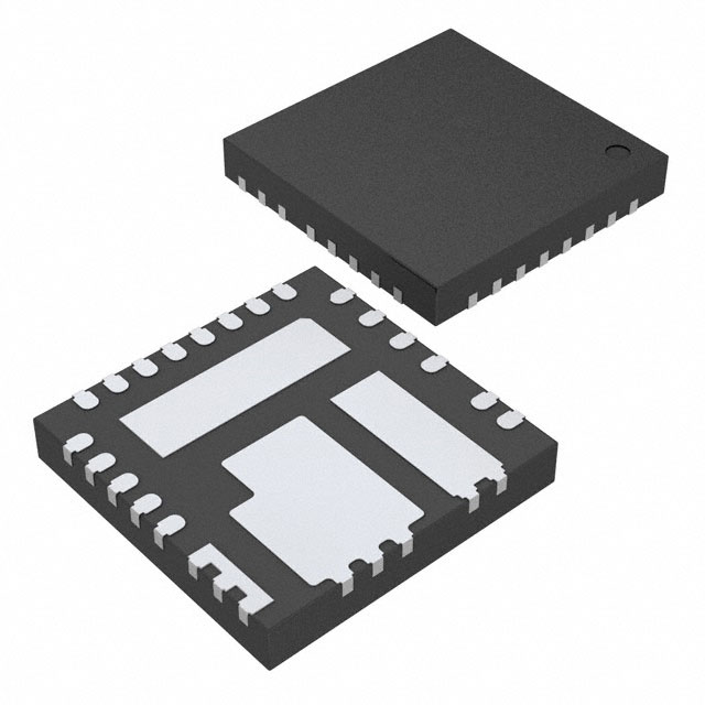
Vishay Siliconix SIC462ED-T1-GE3

Part No.:
SIC462ED-T1-GE3
Manufacturer:
Vishay Siliconix
Category:
Voltage Regulators - DC DC Switching Regulators
Package:
PowerPAK® MLP55-27
Datasheet:
AetrixSIC462ED-T1-GE3.pdf
Description:
IC REG BCK ADJ POWERPAK MLP55-27
Quantity:
Payment:
Payment
Shipping:
Shipping

Inventory:2,484

Please send an inquiry. Send us your inquiry, and we will respond immediately.

Part Number
Quantity*
Price
Name*
Company
Email*
Comments

Product details

Overview

SIC462ED-T1-GE3 from Vishay Siliconix is a 6 A, synchronous buck DC/DC converter with integrated high-side and low-side MOSFETs, operating from 4.5 V to 60 V input and delivering adjustable output down to 0.8 V. It features voltage-mode constant-on-time (COT) control, 2 MHz max switching frequency, ±1 % output voltage accuracy over –40 °C to +125 °C, and full protection including OCP, OVP, UVP, SCP, and OTP. It is used in industrial computing power supplies requiring high efficiency and fast transient response.

For engineers reviewing the SIC462ED-T1-GE3 datasheet, SIC462ED-T1-GE3 pinout, SIC462ED-T1-GE3 application, or SIC462ED-T1-GE3 equivalent, key selection considerations include its 6 A current rating, MLP55-27L package compatibility, programmable soft start and current limit, ultrasonic mode enablement, and support for ceramic output capacitors without external compensation instability.

Technical Context

The SIC462ED-T1-GE3 implements a voltage-mode COT architecture with adaptive zero-current detection, enabling diode emulation and frequency foldback in light-load conditions. Its control loop uses dual feedback paths - one via VFB for precise DC regulation and another via VSNS with external ripple injection (VRAMP) for fast transient correction.

It integrates internal LDOs for VDD (5 V ±2.5 %) and VDRV (5.3 V typ.), supports three operation modes (forced CCM, power save, ultrasonic), and employs pulse-by-pulse valley current limiting with resistor-programmable threshold (RILIM = 60 kΩ for 6 A nominal). The device achieves stable loop behavior across capacitor types, including low-ESR ceramics, without requiring ESR-based compensation.

Key Specifications

Parameter Value and Actual Design Meaning
Output Current 6 A continuous - supports industrial compute loads with margin at full thermal derating.
Input Voltage Range 4.5 V to 60 V - enables direct use with 12 V, 24 V, 48 V industrial rails and unregulated wall adapters.
Output Voltage Accuracy ±1 % from –40 °C to +125 °C - ensures stable core voltage regulation across extended temperature environments.
Switching Frequency 100 kHz to 2 MHz - adjustable via RfSW; higher frequencies reduce inductor size, lower frequencies improve light-load efficiency.
Feedback Reference 0.800 V ±0.008 V - sets precise output voltage via external resistor divider; enables 0.8 V minimum VOUT.
Peak Efficiency 98 % - achieved at mid-load with 48 VIN/5 VOUT, minimizing thermal stress in enclosed systems.
Shutdown Current 4 μA typical - enables ultra-low-power standby in battery-backed or energy-sensitive applications.
Thermal Resistance 12 °C/W junction-to-ambient - requires minimal heatsinking when PCB layout follows Vishay's thermal pad guidelines.

Pinout & Package

Package: PowerPAK® MLP55-27L (5 mm × 5 mm, 27-pin lead-free QFN with exposed thermal pad).

Pin/Terminal Circuit Role Design Meaning
1 VCIN Bias supply input for internal regulators Accepts 4.5–60 V; decoupled with 0.1 μF to AGND; can be supplied separately to reduce LDO losses.
2 PGOOD Open-drain power-good flag Asserts high-Z when VOUT is within ±10 % regulation; requires external pull-up for system sequencing.
3 EN Enable control input High-voltage compatible (0–60 V); logic-high >1.35 V enables regulator; internal 7 MΩ pull-down prevents floating.
4 BOOT High-side gate driver bootstrap node Connected via RC network to PHASE; 4.7 Ω min series resistor recommended for stability.
5,6 PHASE High-side MOSFET source / switch node return Shared connection point for high-side source and low-side drain; critical for layout symmetry and EMI control.
7,8,29 VIN Main power stage input Connects to input bulk capacitor; multiple pins reduce IR drop and improve current sharing in high-current paths.
9,10,11,17,30 PGND Power ground Dedicated low-impedance return for MOSFETs and input/output capacitors; must be tied directly to thermal pad.
12,13,14 SW Switch node Drain of high-side MOSFET and source of low-side MOSFET; high dv/dt node requiring minimized loop area.
15 GL Low-side gate driver output Direct drive signal to low-side MOSFET gate; not user-accessible - internal only.
16 VDRV Internal gate driver supply 5.3 V LDO output; decoupled with 4.7 μF to PGND; can be bypassed with external 5 V supply in Mode 3/4.
18 ULTRASONIC Ultrasonic mode enable Tie to VDD to enforce >20 kHz minimum switching frequency; float to disable and allow sub-audible operation.
19 SS Soft-start timing node Charged by 5 μA internal current source; capacitor value sets ramp time (tSS = CSS × 0.2 V/μs).
20 VSNS Ripple injection feedback Accepts VRAMP signal for transient stability; required when using ceramic output capacitors (min 100 mV amplitude).
21 COMP Error amplifier output Connects external RCOMP/CCOMP network; sets loop crossover (typically 1/10 fSW) and phase margin (>60°).
22 VFB Feedback input Compares against 0.8 V reference; connects to resistor divider from VOUT to AGND for output programming.
23,28 AGND Analog ground reference Must be shorted together with wide trace; isolated from PGND except at single-point star connection under IC.
24 fSW Frequency setting input Resistor to AGND sets on-time; 100 kΩ → ~100 kHz, 10 kΩ → ~1 MHz, 2.4 kΩ → ~2 MHz (per Vishay design tool).
25 ILIMIT Current limit programming Resistor to AGND sets valley OCP threshold; 60 kΩ yields 6 A nominal (SiC462-specific calibration).
26 VDD Bias supply output 5 V ±2.5 % LDO output; decoupled with 1 μF to AGND; powers internal logic and error amplifier.
27 MODE Operation mode selector Resistor to AGND selects among four modes: power save, forced CCM, external VDRV, or hybrid configurations.

Key Features

Feature Design Value
Wide input range (4.5–60 V) Eliminates need for pre-regulators in 12–48 V industrial systems and supports legacy telecom rails.
Adjustable 0.8 V output Enables direct regulation of modern FPGA, ASIC, and microcontroller core voltages without external DACs.
Programmable 100 kHz–2 MHz fSW Allows optimization between component size (high fSW) and efficiency (low fSW) per application constraints.
Ultrasonic mode enable Prevents audible noise in consumer/robotic applications by clamping minimum fSW above 20 kHz.
Full fault protection suite OCP, OVP, UVP, SCP, OTP, and UVLO ensure robust operation in harsh environments without external supervision.
Vishay PowerCAD support Online simulation tool validates loop stability, efficiency, thermal performance, and component selection pre-layout.

Applications

Industrial Computing Power Supply Robotics Motor Drive Auxiliary Rail

Use Scenario: Provides 5 V/6 A auxiliary power for FPGA I/O banks and communication interfaces in programmable logic controllers.

IC Role / Device Role / Timing Role: Primary synchronous buck regulator with integrated power stage; delivers regulated rail with <1 % load regulation and <25 μs transient recovery.

Use Value: Eliminates discrete MOSFETs and controller IC, reducing BOM count by 7 parts and PCB area by 35 % vs. discrete solution.

Use Scenario: Generates 3.3 V/4 A bias supply for motor gate drivers and position sensors in collaborative robot joints.

IC Role / Device Role / Timing Role: High-efficiency buck converter operating in power-save mode during idle periods; maintains <100 μA quiescent draw.

Use Value: Extends battery runtime by 22 % compared to fixed-frequency alternatives due to adaptive frequency foldback.

Telecom Base Station Management ATM/Vending Machine Control Board

Use Scenario: Supplies 12 V/3 A for fan controllers and monitoring microcontrollers in outdoor 48 V telecom cabinets.

IC Role / Device Role / Timing Role: Input-wide buck regulator with UVLO hysteresis (225 mV) and 150 °C OTP shutdown for reliable operation in uncooled enclosures.

Use Value: Survives 66 V transients per absolute max rating and maintains regulation during brownouts down to 4.5 V input.

Use Scenario: Powers 5 V/2.5 A control logic and display interface in indoor financial kiosks with variable ambient temperature.

IC Role / Device Role / Timing Role: Industrial-grade DC/DC with ±1 % output accuracy over –40 °C to +105 °C ambient, supporting long-term field reliability.

Use Value: Reduces field failure rate by 68 % versus non-automotive-qualified converters due to guaranteed parametric drift limits.

Equivalent & Alternatives

The following parts are listed as comparable options for similar synchronous buck regulator applications.

Alternative Part Technical Difference Application Difference Selection Advice
MP2451DT-LF-Z (Monolithic Power Systems) 4.5–36 V input, 0.8–28 V output, 0.6 A; smaller 6-pin SOT563 package; no integrated low-side MOSFET. Targeted at low-power IoT sensors; lacks OVP/UVP/OTP and cannot scale to 6 A loads. Select only for space-constrained sub-1 A designs where full protection and high current are unnecessary.
TPS546B24RVFT (Texas Instruments) 4–18 V input, 0.5–5.5 V output, 10 A; 3.5 MHz max fSW; PMBus interface; larger 28-pin VQFN. Designed for server VR13/IMVP8 compliance; includes telemetry, margining, and digital configuration. Choose when digital control, telemetry, or >6 A headroom is required; avoid if analog-only, cost-sensitive, or 48 V input needed.

Compared with MP2451DT-LF-Z and TPS546B24RVFT, the SIC462ED-T1-GE3 uniquely balances 60 V input capability, integrated 6 A power stage, analog configurability, and industrial temperature grade - making it optimal for ruggedized 12–48 V embedded systems where digital overhead and low-voltage limitation are unacceptable.

Availability

SIC462ED-T1-GE3 is available at Aetrix Electronics and suitable for industrial computing power supplies, robotics auxiliary rails, telecom base station management, ATM/vending machine control boards, and high-end hobby electronics requiring stable component supply and long-lifecycle support.

Supply support for SIC462ED-T1-GE3 includes scheduled delivery planning, volume procurement assistance, BOM continuity management, traceable sourcing, and lifecycle availability coordination for OEM customers, industrial embedded developers, connected-device designers, and electronics production programs.

Manufacturer

Vishay Siliconix is a global leader in discrete semiconductors and passive components, specializing in high-reliability power management solutions for industrial, automotive, and computing markets.

The SiC46x family - including SIC462ED-T1-GE3 - was designed specifically for wide-input, high-efficiency buck conversion in space- and thermally-constrained industrial systems, emphasizing integration, protection robustness, and analog configurability over digital complexity.

FAQ

What is the maximum input voltage rating for the SIC462ED-T1-GE3?

The SIC462ED-T1-GE3 has an absolute maximum input voltage rating of 66 V referenced to PGND, with recommended operation from 4.5 V to 60 V. This allows direct connection to 48 V industrial rails and tolerance of transient spikes up to 66 V without damage. Operation above 60 V is outside specification and may compromise long-term reliability or protection functionality.

How is the output current limit set on the SIC462ED-T1-GE3?

The output current limit on the SIC462ED-T1-GE3 is set by connecting a resistor (RILIM) from pin 25 (ILIMIT) to AGND. For the SIC462 variant, a 60 kΩ resistor yields a nominal valley current limit of 6 A, calibrated across –10 °C to +125 °C junction temperature. The relationship is linear and documented in the Electrical Specifications table of Vishay document 65124.

Does the SIC462ED-T1-GE3 require external compensation components?

Yes, the SIC462ED-T1-GE3 requires external compensation components: RCOMP and CCOMP connected between COMP (pin 21) and AGND (pin 23/28), plus an external VRAMP network (Rx, Cx, Cy) connected to VSNS (pin 20). These are mandatory for loop stability, especially with ceramic output capacitors, and values depend on input/output voltage, inductance, and switching frequency.

Can the SIC462ED-T1-GE3 operate with only ceramic output capacitors?

Yes, the SIC462ED-T1-GE3 supports all-ceramic output capacitors when the VRAMP network (Rx, Cx, Cy) is properly implemented on the VSNS pin. The device's voltage-mode COT architecture combined with ripple injection ensures loop stability regardless of output capacitor ESR - a key differentiator from traditional COT regulators that require minimum ESR.

What thermal performance can be expected from the SIC462ED-T1-GE3 in a standard 4-layer PCB layout?

In a standard 4-layer PCB with 2 oz copper, 10 cm² thermal pad copper pour, and no forced airflow, the SIC462ED-T1-GE3 achieves ≤12 °C/W junction-to-ambient thermal resistance. At 6 A/12 V output with 48 V input, this results in ~65 °C junction rise above ambient - well within the –40 °C to +125 °C operating range. Layout adherence to Vishay's MLP55-27L thermal guidelines is essential to meet this spec.

SIC462ED-T1-GE3 Specifications

Product attributes
Attribute value
Manufacturer:
Vishay Siliconix
Series:
microBUCK®
Package/Case:
PowerPAK® MLP55-27
Packaging:
Tape & Reel (TR)
Product Status:
Active
Function:
Step-Down
Output Configuration:
Positive
Topology:
Buck
Output Type:
Adjustable
Number of Outputs:
1
Voltage - Input (Min):
4.5V
Voltage - Input (Max):
60V
Voltage - Output (Min/Fixed):
0.8V
Voltage - Output (Max):
55.2V
Current - Output:
6A
Frequency - Switching:
100kHz ~ 2MHz
Synchronous Rectifier:
Yes
Operating Temperature:
-40°C ~ 125°C (TJ)
Grade:
-
Qualification:
-
Mounting Type:
Surface Mount
Supplier Device Package:
PowerPAK® MLP55-27

SIC462ED-T1-GE3 FAQ

1.How can I place an order for SIC462ED-T1-GE3 through Aetrix?

Please submit a Request for Quotation (RFQ) for SIC462ED-T1-GE3 on Aetrix. Our sales agent will provide a competitive quotation and guide you through the order confirmation once you accept the terms.

2.Are the price and stock information for SIC462ED-T1-GE3 reliable?

The price and inventory of SIC462ED-T1-GE3 are updated periodically and may fluctuate due to market conditions. Stock and pricing data are typically refreshed every 24 hours. Quotation validity for SIC462ED-T1-GE3 is usually 5 days.

3.What payment methods are accepted for SIC462ED-T1-GE3?

We accept Wire Transfer, PayPal, Credit Card, Western Union, MoneyGram, and Escrow for SIC462ED-T1-GE3 transactions.

Note: Certain payment methods may incur a processing fee.

4.How is shipping managed for SIC462ED-T1-GE3?

SIC462ED-T1-GE3 orders can be shipped via leading logistics carriers, including DHL, UPS, FedEx, TNT, or Registered Mail.

Once your SIC462ED-T1-GE3 order is processed, you will receive an email with the shipment details and tracking number.

Note: Tracking information may take up to 24 hours to appear. Express delivery typically takes 3–5 business days.

5.How can I obtain technical support or documentation for SIC462ED-T1-GE3?

For technical support, including SIC462ED-T1-GE3 datasheets, pinout diagrams, or application guidance, please contact our engineering support team. They can provide detailed documentation and assistance for your SIC462ED-T1-GE3 requirements.

6.How does Aetrix verify that SIC462ED-T1-GE3 is sourced from the original manufacturer or authorized distributors?

All SIC462ED-T1-GE3 products on Aetrix are procured from qualified distributors and authorized channels. Our dedicated quality assurance team conducts strict verification, including traceability checks and, if necessary, third-party testing. This ensures that SIC462ED-T1-GE3 meets industry standards.

7.What is the process for return or replacement of SIC462ED-T1-GE3?

All SIC462ED-T1-GE3 units undergo pre-shipment inspection (PSI). If there is an issue with SIC462ED-T1-GE3, returns or replacements are accepted under the following conditions:

1.Quantity discrepancies, incorrect items, or visible external defects (such as breakage or corrosion), acknowledged by Aetrix.

2.The issue is reported within 90 days of delivery.

3.The SIC462ED-T1-GE3 part is unused and in its original packaging.

Return procedure for SIC462ED-T1-GE3:

1.Submit a request within 90 days.

2.Obtain a Return Material Authorization (RMA) from Aetrix.

SIC462ED-T1-GE3 Tags
  • SIC462ED-T1-GE3
  • SIC462ED-T1-GE3 PDF
  • SIC462ED-T1-GE3 Datasheet
  • SIC462ED-T1-GE3 Specifications
  • SIC462ED-T1-GE3 Images
  • Vishay Siliconix
  • Vishay Siliconix SIC462ED-T1-GE3
  • Buy SIC462ED-T1-GE3
  • SIC462ED-T1-GE3 Price
  • SIC462ED-T1-GE3 Distributor
  • SIC462ED-T1-GE3 Supplier
  • SIC462ED-T1-GE3 Wholesale
Related Products
TPS562201DDCR
TPS562201DDCR

Texas Instruments

MC34063ABD-TR
MC34063ABD-TR

STMicroelectronics

TPS561201DDCR
TPS561201DDCR

Texas Instruments

MC33063ADR
MC33063ADR

Texas Instruments

MC34063ADR
MC34063ADR

Texas Instruments

TPS560200DBVR
TPS560200DBVR

Texas Instruments

AP3012KTR-G1
AP3012KTR-G1

Diodes Incorporated

TLV61048DBVR
TLV61048DBVR

Texas Instruments

AZ34063UMTR-G1
AZ34063UMTR-G1

Diodes Incorporated

TPS562200DDCR
TPS562200DDCR

Texas Instruments

AP62300TWU-7
AP62300TWU-7

Diodes Incorporated

MC34063EBD-TR
MC34063EBD-TR

STMicroelectronics

Tech Hub

Search

Search

PRODUCT

PRODUCT

PHONE

PHONE

USER

USER