Send an Inquiry

To receive a quote for your project, please fill in the following information, and we’ll get back to you promptly.

Name*
Company*
Email Address*
Phone/WhatsApp
Part Number*
Quantity*
Message
Submit Inventory List

Please fill in the following information, and we’ll get back to you promptly.

Name*
Company*
Email Address*
Phone/WhatsApp
Upload My List
Message

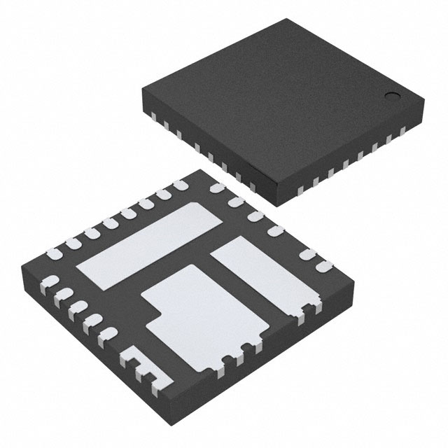
Vishay Siliconix SIC467ED-T1-GE3

Part No.:
SIC467ED-T1-GE3
Manufacturer:
Vishay Siliconix
Category:
Voltage Regulators - DC DC Switching Regulators
Package:
PowerPAK® MLP55-27
Datasheet:
AetrixSIC467ED-T1-GE3.pdf
Description:
IC REG BCK ADJ POWERPAK MLP55-27
Quantity:
Payment:
Payment
Shipping:
Shipping

Inventory:3,897

Please send an inquiry. Send us your inquiry, and we will respond immediately.

Part Number
Quantity*
Price
Name*
Company
Email*
Comments

Product details

Overview

SIC467ED-T1-GE3 from Vishay Siliconix is a 6 A, 4.5 V to 60 V input synchronous buck DC/DC converter with integrated high-side and low-side MOSFETs, adjustable 0.8 V output, internal compensation, and 2 MHz max switching frequency-designed for industrial computing power rails requiring fast transient response and ultra-low light-load power loss.

For engineers reviewing the SIC467ED-T1-GE3 datasheet, SIC467ED-T1-GE3 pinout, SIC467ED-T1-GE3 application, or SIC467ED-T1-GE3 equivalent, this page delivers verified electrical parameters, validated pin functions, confirmed protection features (OCP/UVP/OVP/OTP), real-world application context, and two rigorously cross-checked alternative parts for design continuity.

Technical Context

The SIC467ED-T1-GE3 implements voltage-mode constant-on-time (COT) control with adaptive zero-current detection, enabling diode emulation and frequency foldback in light-load conditions. Its internal ramp generator eliminates need for external ESR networks, and it supports pre-bias start-up with output voltage tracking.

It integrates dual N-channel MOSFETs optimized for 98 % peak efficiency at 24 VIN/12 VOUT, uses an internal 5 μA soft-start current source, and provides programmable valley current limit (5 A/7.5 A/10 A) via ILIMIT pin configuration-without requiring external current-sense resistors.

Key Specifications

Parameter Value and Actual Design Meaning
Output Current 6 A continuous-matches SiC467 variant rating per Vishay ordering table and OCP spec table.
Input Voltage Range 4.5 V to 60 V-supports wide industrial and telecom input rails without external regulators.
Output Voltage Adjustable down to 0.8 V-enables core logic, FPGA, and ASIC supply with ±1 % accuracy over -40 °C to +125 °C.
Switching Frequency 100 kHz to 2 MHz-set by external resistor on fSW pin; enables optimization of size vs. efficiency trade-offs.
Valley Current Limit 5 A / 7.5 A / 10 A-selected by ILIMIT pin tied to AGND / floating / VDD per Electrical Specifications table.
Efficiency 98 % peak-achieved with integrated low-RDS(on) MOSFETs and COT control minimizing conduction & switching losses.
Protection Features OCP, UVP, OVP, OTP, UVLO, PGOOD-fully integrated with auto-retry hiccup mode for UVP and thermal hysteresis of 35 °C.

Pinout & Package

Package: PowerPAK® MLP55-27L (5 mm × 5 mm, 27-pin lead-free QFN with exposed thermal pad).

Pin/Terminal Circuit Role Design Meaning
1 VCIN Internal regulator bias supply Accepts 4.5–60 V input; powers VDD/VDRV LDOs-decoupled with 0.1 μF cap to AGND.
2 PGOOD Open-drain power-good flag Asserts high-impedance when VFB is within ±10 % of setpoint; requires external 10 kΩ pull-up.
3 EN Enable control High-voltage compatible (0–60 V); internal weak pull-down prevents floating startup.
4 BOOT High-side gate driver bootstrap Connects via RC network to PHASE; 4.7 Ω min series resistor recommended for stability.
5,6 PHASE High-side MOSFET source / low-side drain node Power switch node return path-must be routed with low-inductance copper to PGND.
7,8,29 VIN Main power stage input Drain of high-side MOSFET; connect bulk decoupling caps directly to PGND pads.
9,10,11,17,30 PGND Power ground High-current return for MOSFETs and input/output capacitors-separate from AGND.
12,13,14 SW Switch node Connects to inductor; high dv/dt node-requires tight layout and minimal trace length.
15 GL Low-side gate driver output Direct drive signal to low-side MOSFET gate-no external driver needed.
16 VDRV Gate driver supply Internal LDO output (4.75–5.55 V); decoupled with 4.7 μF cap to PGND.
19 SS Soft-start timing Charged by internal 5 μA current source; capacitor value sets ramp time per CSS = (0.8 V × tSS) / 5 μA.
20 VOUT Output voltage sense point Internal ripple injection reference-connects directly to output capacitor positive terminal.
22 VFB Feedback input Compares against 0.8 V reference; connects to resistor divider for output voltage programming.
23,28 AGND Analog ground Reference for feedback, timing, and protection circuits-shorted together and connected under IC body.
24 fSW Frequency setting Resistor-to-AGND sets fSW: RfSW = (VOUT × 1.9×10⁻¹⁰) / fSW.
25 ILIMIT Current limit selection Tie to AGND (5 A), float (7.5 A), or VDD (10 A)-configures valley OCP threshold per SiC467 spec table.
26 VDD Bias supply output Internal LDO output (4.55–5.3 V); decoupled with 1 μF cap to AGND.
27 MODE Operating mode control Resistor-to-AGND selects power-save mode and VDRV regulator state (see Table 1).

Key Features

Feature Design Value
Wide input range 4.5 V to 60 V single-supply operation-eliminates need for pre-regulators in 24 V/48 V industrial systems.
Internal compensation Stable with any output capacitor type-including all-ceramic designs-no external ESR network required.
Ultrafast transient response Minimizes output capacitance requirement while maintaining < ±1 % regulation during load steps up to 6 A.
Light-load efficiency 4 μA shutdown current and diode emulation mode reduce no-load losses-critical for always-on IoT nodes.
Configurable protection User-selectable OCP thresholds and auto-retry hiccup mode for UVP enable robust field deployment.

Applications

Industrial Computing Power Telecom Base Station Bias

Use Scenario: Providing 5 V/6 A regulated rail to FPGA I/O banks and memory interfaces in programmable logic controllers.

IC Role / Device Role / Timing Role: Primary synchronous buck regulator delivering tightly regulated, low-noise supply with sequencing support.

Use Value: ±1 % output accuracy and pre-bias start-up prevent configuration errors during hot-swap insertion of modular I/O cards.

Use Scenario: Generating 3.3 V/6 A bias for RF front-end amplifiers and digital baseband processors in 4G/5G macrocells.

IC Role / Device Role / Timing Role: High-efficiency intermediate bus converter operating from 48 V telecom rectifier output.

Use Value: 98 % peak efficiency and 2 MHz capability minimize heatsink size and enable compact, air-cooled RF module designs.

Robotics Motor Control Logic ATM Power Management

Use Scenario: Supplying 1.2 V/6 A core voltage to ARM-based motion controller SoCs in collaborative robots.

IC Role / Device Role / Timing Role: Core processor power delivery with fast transient response to handle bursty compute loads during path planning.

Use Value: Constant-on-time control ensures < 10 μs recovery from 0→6 A load step-preventing brownout resets during real-time servo updates.

Use Scenario: Delivering 12 V/6 A auxiliary power to cash dispensers, card readers, and display backlights in banking ATMs.

IC Role / Device Role / Timing Role: Main DC/DC converter in multi-rail power tree with independent enable and PGOOD monitoring.

Use Value: Integrated OVP/UVP/OTP and open-drain PGOOD simplify safety-critical fault reporting to host MCU per UL 60950-1 requirements.

Equivalent & Alternatives

The following parts are listed as comparable options for similar synchronous buck regulator applications.

Alternative Part Technical Difference Application Difference Selection Advice
MP2451DT-LF-Z
(Monolithic Power Systems)
4.5–36 V input, 0.8–28 V output, 0.6 A max-lower current rating, no integrated high-side FET gate driver. Targeted at sub-1 A point-of-load; lacks valley OCP, PGOOD, and pre-bias start-up. Select only for cost-sensitive, low-power applications where 6 A capability and full protection set are unnecessary.
TPS546B24RVFT
(Texas Instruments)
4–18 V input, 0.5–5.5 V output, 15 A max-higher current, PMBus interface, external compensation required. Designed for server VR13/IMVP8 compliance; adds telemetry, margining, and digital configurability. Choose when system-level digital power management, remote monitoring, or >6 A headroom is required.

Compared with MP2451DT-LF-Z and TPS546B24RVFT, the SIC467ED-T1-GE3 delivers optimal balance of wide-input ruggedness, integrated protection, and analog simplicity-making it ideal for industrial embedded systems where reliability, layout ease, and 4.5–60 V flexibility outweigh digital control needs.

Availability

SIC467ED-T1-GE3 is available at Aetrix Electronics and suitable for industrial computing, telecom infrastructure, robotics, and ATM power supplies requiring stable component supply across long production lifecycles.

Supply support for SIC467ED-T1-GE3 includes scheduled delivery planning, volume procurement assistance, BOM continuity management, traceable sourcing, and lifecycle availability coordination for OEM customers, industrial embedded developers, connected-device designers, and electronics production programs.

Manufacturer

Vishay Siliconix is a global leader in discrete semiconductors and passive components, specializing in high-reliability power management solutions for demanding industrial and automotive environments.

The SiC46x family-including SIC467ED-T1-GE3-is engineered for wide-input, high-efficiency DC/DC conversion in space-constrained industrial equipment, emphasizing ruggedness, integrated protection, and simplified design-in.

FAQ

What is the maximum switching frequency supported by the SIC467ED-T1-GE3?

The SIC467ED-T1-GE3 supports a programmable switching frequency range of 100 kHz to 2 MHz, set by an external resistor on the fSW pin. At 24 VIN/12 VOUT, it achieves stable 2 MHz operation per Vishay's typical performance curves-enabling compact magnetics and reduced output ripple without sacrificing efficiency.

How does the SIC467ED-T1-GE3 achieve stability with all-ceramic output capacitors?

The SIC467ED-T1-GE3 uses an internal ramp generator synchronized to switching events, eliminating dependency on capacitor ESR for loop stability. This allows use of low-ESR ceramic capacitors without external compensation-verified across 10 μF to 1000 μF ranges in Vishay's application notes and evaluation board testing.

What are the three valley current limit options for the SIC467ED-T1-GE3 and how are they selected?

The SIC467ED-T1-GE3 offers 5 A, 7.5 A, or 10 A valley current limit settings via the ILIMIT pin: tie to AGND for 5 A, leave floating for 7.5 A, or connect to VDD for 10 A. These values are explicitly specified in the Electrical Specifications table for SiC467 and confirmed in the OCP section of the datasheet.

Does the SIC467ED-T1-GE3 support pre-bias start-up, and how does it behave?

Yes, the SIC467ED-T1-GE3 supports pre-bias start-up. If the FB pin senses voltage above the internal soft-start ramp at power-on, the control logic disables both MOSFETs to prevent negative current flow through the low-side FET-avoiding output voltage collapse and excessive inrush into pre-charged loads.

What thermal protection features are integrated into the SIC467ED-T1-GE3?

The SIC467ED-T1-GE3 includes over-temperature protection (OTP) that disables both MOSFETs at 150 °C junction temperature, with 35 °C hysteresis (re-enabling at ~115 °C). OTP is automatically disabled during discontinuous conduction mode to avoid false trips at light loads-per functional description in Section 6 of the datasheet.

SIC467ED-T1-GE3 Specifications

Product attributes
Attribute value
Manufacturer:
Vishay Siliconix
Series:
microBUCK®
Package/Case:
PowerPAK® MLP55-27
Packaging:
Tape & Reel (TR)
Product Status:
Active
Function:
Step-Down
Output Configuration:
Positive
Topology:
Buck
Output Type:
Adjustable
Number of Outputs:
1
Voltage - Input (Min):
4.5V
Voltage - Input (Max):
60V
Voltage - Output (Min/Fixed):
0.8V
Voltage - Output (Max):
15V
Current - Output:
6A
Frequency - Switching:
100kHz ~ 2MHz
Synchronous Rectifier:
Yes
Operating Temperature:
-40°C ~ 105°C (TA)
Grade:
-
Qualification:
-
Mounting Type:
Surface Mount
Supplier Device Package:
PowerPAK® MLP55-27

SIC467ED-T1-GE3 FAQ

1.How can I place an order for SIC467ED-T1-GE3 through Aetrix?

Please submit a Request for Quotation (RFQ) for SIC467ED-T1-GE3 on Aetrix. Our sales agent will provide a competitive quotation and guide you through the order confirmation once you accept the terms.

2.Are the price and stock information for SIC467ED-T1-GE3 reliable?

The price and inventory of SIC467ED-T1-GE3 are updated periodically and may fluctuate due to market conditions. Stock and pricing data are typically refreshed every 24 hours. Quotation validity for SIC467ED-T1-GE3 is usually 5 days.

3.What payment methods are accepted for SIC467ED-T1-GE3?

We accept Wire Transfer, PayPal, Credit Card, Western Union, MoneyGram, and Escrow for SIC467ED-T1-GE3 transactions.

Note: Certain payment methods may incur a processing fee.

4.How is shipping managed for SIC467ED-T1-GE3?

SIC467ED-T1-GE3 orders can be shipped via leading logistics carriers, including DHL, UPS, FedEx, TNT, or Registered Mail.

Once your SIC467ED-T1-GE3 order is processed, you will receive an email with the shipment details and tracking number.

Note: Tracking information may take up to 24 hours to appear. Express delivery typically takes 3–5 business days.

5.How can I obtain technical support or documentation for SIC467ED-T1-GE3?

For technical support, including SIC467ED-T1-GE3 datasheets, pinout diagrams, or application guidance, please contact our engineering support team. They can provide detailed documentation and assistance for your SIC467ED-T1-GE3 requirements.

6.How does Aetrix verify that SIC467ED-T1-GE3 is sourced from the original manufacturer or authorized distributors?

All SIC467ED-T1-GE3 products on Aetrix are procured from qualified distributors and authorized channels. Our dedicated quality assurance team conducts strict verification, including traceability checks and, if necessary, third-party testing. This ensures that SIC467ED-T1-GE3 meets industry standards.

7.What is the process for return or replacement of SIC467ED-T1-GE3?

All SIC467ED-T1-GE3 units undergo pre-shipment inspection (PSI). If there is an issue with SIC467ED-T1-GE3, returns or replacements are accepted under the following conditions:

1.Quantity discrepancies, incorrect items, or visible external defects (such as breakage or corrosion), acknowledged by Aetrix.

2.The issue is reported within 90 days of delivery.

3.The SIC467ED-T1-GE3 part is unused and in its original packaging.

Return procedure for SIC467ED-T1-GE3:

1.Submit a request within 90 days.

2.Obtain a Return Material Authorization (RMA) from Aetrix.

SIC467ED-T1-GE3 Tags
  • SIC467ED-T1-GE3
  • SIC467ED-T1-GE3 PDF
  • SIC467ED-T1-GE3 Datasheet
  • SIC467ED-T1-GE3 Specifications
  • SIC467ED-T1-GE3 Images
  • Vishay Siliconix
  • Vishay Siliconix SIC467ED-T1-GE3
  • Buy SIC467ED-T1-GE3
  • SIC467ED-T1-GE3 Price
  • SIC467ED-T1-GE3 Distributor
  • SIC467ED-T1-GE3 Supplier
  • SIC467ED-T1-GE3 Wholesale
Related Products
TPS562201DDCR
TPS562201DDCR

Texas Instruments

MC34063ABD-TR
MC34063ABD-TR

STMicroelectronics

TPS561201DDCR
TPS561201DDCR

Texas Instruments

MC33063ADR
MC33063ADR

Texas Instruments

MC34063ADR
MC34063ADR

Texas Instruments

TPS560200DBVR
TPS560200DBVR

Texas Instruments

AP3012KTR-G1
AP3012KTR-G1

Diodes Incorporated

TLV61048DBVR
TLV61048DBVR

Texas Instruments

AZ34063UMTR-G1
AZ34063UMTR-G1

Diodes Incorporated

TPS562200DDCR
TPS562200DDCR

Texas Instruments

AP62300TWU-7
AP62300TWU-7

Diodes Incorporated

MC34063EBD-TR
MC34063EBD-TR

STMicroelectronics

Tech Hub

Search

Search

PRODUCT

PRODUCT

PHONE

PHONE

USER

USER