Send an Inquiry

To receive a quote for your project, please fill in the following information, and we’ll get back to you promptly.

Name*
Company*
Email Address*
Phone/WhatsApp
Part Number*
Quantity*
Message
Submit Inventory List

Please fill in the following information, and we’ll get back to you promptly.

Name*
Company*
Email Address*
Phone/WhatsApp
Upload My List
Message

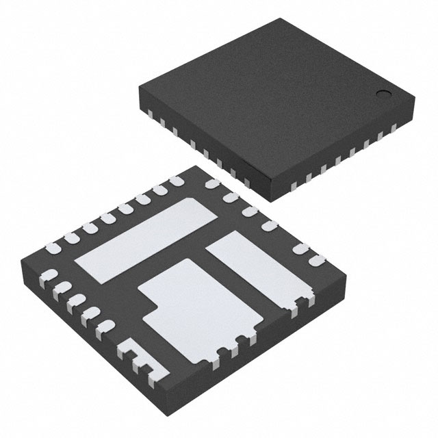
Vishay Siliconix SIC474ED-T1-GE3

Part No.:
SIC474ED-T1-GE3
Manufacturer:
Vishay Siliconix
Category:
Voltage Regulators - DC DC Switching Regulators
Package:
PowerPAK® MLP55-27
Datasheet:
AetrixSIC474ED-T1-GE3.pdf
Description:
IC REG BCK ADJ POWERPAK MLP55-27
Quantity:
Payment:
Payment
Shipping:
Shipping

Inventory:16,509

Please send an inquiry. Send us your inquiry, and we will respond immediately.

Part Number
Quantity*
Price
Name*
Company
Email*
Comments

Product details

Overview

SIC474ED-T1-GE3 from Vishay Siliconix is a 3 A, 4.5 V to 55 V input synchronous buck DC/DC converter with integrated high-side and low-side MOSFETs, adjustable 0.8 V output, and voltage-mode constant-on-time (COT) control-designed for industrial computing, robotics, and battery-powered systems requiring compact, high-efficiency point-of-load regulation.

For engineers reviewing the SIC474ED-T1-GE3 datasheet, SIC474ED-T1-GE3 pinout, SIC474ED-T1-GE3 application, or SIC474ED-T1-GE3 equivalent, key selection criteria include its 3 A continuous current rating, 98 % peak efficiency, ±1 % output voltage accuracy over –40 °C to +125 °C, programmable 100 kHz–2 MHz switching frequency, and robust protection suite including OCP, OVP, UVP, OTP, and PGOOD.

Technical Context

The SIC474ED-T1-GE3 implements a voltage-mode COT architecture with adaptive zero-current detection, enabling fast transient response and stable operation with ceramic output capacitors without external ESR requirements. Its control loop uses dual feedback paths: steady-state regulation via VFB (0.8 V reference) and feed-forward transient correction via VSNS with externally injected ripple (VRAMP).

It integrates a 37 mΩ high-side and 27 mΩ low-side n-channel MOSFET pair optimized for 3 A continuous output, supports three operating modes (forced CCM, power-save, ultrasonic), and features user-programmable soft start, current limit, and switching frequency-all configured via external resistors and capacitors connected to dedicated pins (SS, ILIMIT, fSW, MODE, ULTRASONIC).

Key Specifications

Parameter Value and Actual Design Meaning
Input Voltage Range 4.5 V to 55 V - supports wide-range industrial, telecom, and battery-derived rails without pre-regulation.
Output Current 3 A continuous - matches SiC474 variant within pin-compatible SiC47x family (vs. 5 A/8 A/12 A siblings).
Output Voltage Adjustable down to 0.8 V - set via external resistor divider on VFB; ±1 % accuracy over full temperature range ensures tight regulation in precision loads.
Switching Frequency 100 kHz to 2 MHz - programmed via resistor on fSW pin; enables optimization of size (high-f) vs. efficiency (low-f) and EMI compliance.
Peak Efficiency 98 % - achieved using integrated low-RDS(on) MOSFETs (37 mΩ HS / 27 mΩ LS) and adaptive gate drive.
Protection Features OCP (4–6 A threshold), OVP (+20 %), UVP (–80 %), OTP (150 °C trip), PGOOD flag - enables autonomous fault recovery and system-level monitoring without external circuitry.
Control Architecture Voltage-mode COT with VRAMP injection - eliminates need for output capacitor ESR, supports ultra-low-ESR ceramics, and delivers <100 ns minimum off-time for light-load stability.

Pinout & Package

Package: PowerPAK® MLP55-27L - 5 mm × 5 mm, 27-pin lead (Pb)-free power-enhanced QFN with exposed thermal pad; optimized for high-power density and thermal performance in space-constrained PCB layouts.

Pin/Terminal Circuit Role Design Meaning
1 VCIN Internal regulator supply input Bias source for VDD/VDRV LDOs; can be tied to VIN or separate ≥5 V rail to reduce linear regulator losses.
2 PGOOD Open-drain power-good indicator Signals valid output regulation (VFB > 0.8 V + 20 %); requires external pull-up for system sequencing or fault reporting.
3 EN Enable control input High-voltage compatible (0–55 V); internal 5 MΩ pull-down prevents floating; logic-high >1.35 V enables regulation.
4 BOOT High-side gate driver bootstrap Provides floating supply for HS MOSFET gate drive; requires external 0.1 μF ceramic capacitor to PHASE.
5,6 PHASE Power stage switch node return Low-inductance path for HS gate driver return; must be routed with minimal loop area to reduce EMI and ringing.
7,8,29 VIN Main power stage input Connects to bulk input capacitor; shared with VCIN unless separate bias is used; rated to 60 V absolute max.
9–11,17,30 PGND Power ground High-current return path for MOSFETs and input/output capacitors; must be solidly connected to thermal pad.
12–14 SW Switch node Drain connection of HS MOSFET and source of LS MOSFET; critical high-dv/dt node requiring short, low-inductance routing to inductor.
15 GL Low-side gate driver output Direct drive signal for LS MOSFET gate; not user-accessible-internal only.
16 VDRV Gate driver supply output LDO output (5.3 V typ.) for HS/LS gate drive; decoupled with 4.7 μF to PGND; can be bypassed with external 5 V supply in Mode 3/4.
18 ULTRASONIC Ultrasonic mode enable Tie to VDD to enforce >20 kHz min. switching in DCM; float to disable and allow sub-audible operation for ultra-low-noise applications.
19 SS Soft-start timing Internal 5 μA current charges external capacitor to ramp VOUT linearly; sets inrush current limit and startup timing.
20 VSNS Ripple injection feedback Accepts externally generated VRAMP signal (100–900 mV) to stabilize COT control with ceramic capacitors.
21 COMP Error amplifier output Connects external RCOMP/CCOMP network to set loop gain, phase margin, and transient response.
22 VFB Feedback input Monitors output via resistor divider; compares to 0.8 V internal reference; ±1 % accuracy enables precise output setting.
23,28 AGND Analog ground Reference for VFB, COMP, VSNS, MODE, ILIMIT, fSW, SS; must be isolated from PGND except at single-point star ground.
24 fSW Frequency programming Resistor-to-AGND sets switching frequency (100 kHz–2 MHz); enables EMI tuning and efficiency optimization.
25 ILIMIT Current limit programming Resistor-to-AGND sets valley OCP threshold (4–6 A for SIC474); provides scalable overcurrent protection.
26 VDD Bias supply output LDO output (5 V typ.) for internal logic; decoupled with 1 μF to AGND; UVLO threshold 4.25 V ensures reliable startup.
27 MODE Operating mode selection Resistor-to-AGND selects among four configurations: power-save, forced CCM, or external VDRV options-enabling fine-grained efficiency vs. noise trade-offs.

Key Features

Feature Design Value
Wide 4.5 V–55 V input range Eliminates need for intermediate pre-regulators in 12 V, 24 V, 48 V, and battery-based systems (e.g., robotics, industrial PLCs).
Integrated 37 mΩ/27 mΩ MOSFETs Reduces BOM count and layout complexity while delivering 98 % peak efficiency at 12 VIN/5 VOUT.
Programmable 100 kHz–2 MHz fSW Enables EMI spread-spectrum design, compact magnetics, and optimal efficiency across load conditions.
Ultrafast transient response Stabilizes output with minimal output capacitance (e.g., 2 × 22 μF X5R) due to COT + VRAMP architecture.
Full fault protection suite OCP, OVP, UVP, OTP, and PGOOD enable autonomous operation in unattended equipment (e.g., vending machines, ATMs).
Three selectable operating modes Forced CCM (low noise), power-save (high light-load efficiency), or ultrasonic (>20 kHz) - configurable without firmware changes.

Applications

Industrial Computing Robotics & Motion Control

Use Scenario: Point-of-load regulation for FPGA I/O banks and microcontroller cores in programmable logic controllers (PLCs) and edge AI gateways.

IC Role / Device Role / Timing Role: Primary synchronous buck regulator delivering stable 1.2 V/3 A or 3.3 V/3 A from 24 V or 48 V backplane.

Use Value: ±1 % output accuracy and fast transient response prevent logic errors during burst-mode processing; integrated MOSFETs reduce board area by >40 % vs. controller+discrete solution.

Use Scenario: Powering motor drivers, sensor interfaces, and MCU subsystems in collaborative robots and autonomous mobile platforms.

IC Role / Device Role / Timing Role: High-efficiency 5 V/3 A supply for servo control ICs and IMU sensors, operating from 12 V Li-ion battery packs.

Use Value: 98 % peak efficiency extends runtime; ultrasonic mode eliminates audible coil whine during low-speed positioning; PGOOD enables safe motion startup sequence.

Networking Equipment Power Tools & Portable Devices

Use Scenario: Intermediate 5 V rail generation in 5G small cell base stations and Ethernet switches powered from 48 V PoE++ infrastructure.

IC Role / Device Role / Timing Role: Secondary buck converter stepping 48 V to 5 V for PHY transceivers, management controllers, and fan drivers.

Use Value: 55 V absolute max input withstands load-dump transients; thermal shutdown (150 °C) protects against airflow blockage in sealed enclosures.

Use Scenario: Compact 12 V/3 A supply for brushless motor controllers and digital displays in cordless drills, saws, and garden tools.

IC Role / Device Role / Timing Role: Main DC/DC stage converting 18–21 V battery stack to regulated 12 V for motor gate drivers and logic.

Use Value: 3 A capability supports peak motor currents; ruggedized MLP55-27L package withstands mechanical shock and vibration; OVP/UVP prevents damage during battery swap events.

Equivalent & Alternatives

The following parts are listed as comparable options for similar synchronous buck regulator applications.

Alternative Part Technical Difference Application Difference Selection Advice
MP2451DT-LF-Z (Monolithic Power Systems) 3 A, 4.5–36 V input, fixed 5 V or adjustable output; no integrated VRAMP support; lower max input voltage. Best suited for 24 V systems without 48 V/55 V requirement; lacks ultrasonic mode and programmable OCP. Select when cost sensitivity outweighs input range and advanced protection needs; verify loop stability with ceramic caps without VRAMP.
TPS54331DR (Texas Instruments) 3 A, 3.5–28 V input, adjustable 0.8 V output; current-mode control; no integrated MOSFETs (external FETs required). Requires external high-side/low-side MOSFETs and driver; higher BOM count and layout effort; wider temp range (–40 °C to +150 °C). Choose when higher junction temperature rating or discrete FET selection flexibility is mandatory; accept added complexity for thermal margin.

Compared with MP2451DT-LF-Z and TPS54331DR, the SIC474ED-T1-GE3 offers broader 4.5–55 V input coverage, integrated MOSFETs with lower RDS(on), and unique VRAMP-based COT stability-making it superior for 48 V industrial, telecom, and battery-powered designs demanding compactness, efficiency, and robust fault handling.

Availability

SIC474ED-T1-GE3 is available at Aetrix Electronics and suitable for industrial computing, robotics, and networking equipment requiring stable component supply, long-term lifecycle support, and consistent parametric performance across production batches.

Supply support for SIC474ED-T1-GE3 includes scheduled delivery planning, volume procurement assistance, BOM continuity management, traceable sourcing, and lifecycle availability coordination for OEM customers, industrial embedded developers, connected-device designers, and electronics production programs.

Manufacturer

Vishay Siliconix is a global leader in discrete semiconductors and passive components, specializing in high-reliability power management solutions for industrial, automotive, and computing markets.

The SiC47x product line was designed specifically for high-density, wide-input-voltage DC/DC conversion in space-constrained industrial and embedded systems-emphasizing integration, efficiency, and protection without sacrificing configurability.

FAQ

What is the maximum input voltage rating for the SIC474ED-T1-GE3?

The SIC474ED-T1-GE3 has an absolute maximum input voltage rating of 60 V on VIN and VCIN pins, with recommended operating input range specified as 4.5 V to 55 V. Operation above 55 V is not guaranteed and may trigger overvoltage stress conditions. The device's internal MOSFETs and gate drivers are characterized for reliable performance up to 55 V under normal operating conditions per Vishay's datasheet revision A.

How does the SIC474ED-T1-GE3 achieve stable regulation with ceramic output capacitors?

The SIC474ED-T1-GE3 achieves stable regulation with ceramic capacitors through its voltage-mode constant-on-time (COT) architecture combined with external VRAMP injection via the VSNS pin. Unlike conventional COT regulators, it requires a controlled ripple signal (100–900 mV amplitude) generated by an external Rx/Cx/Cy network to ensure loop stability, eliminate subharmonic oscillation, and maintain fast transient response without relying on capacitor ESR.

What is the current limit threshold for the SIC474ED-T1-GE3, and how is it set?

The SIC474ED-T1-GE3 has a valley current limit threshold of 4 A (min), 5 A (typ), and 6 A (max) at TJ = –10 °C to +125 °C, set by connecting a resistor (RILIM) between ILIMIT pin and AGND. With RILIM = 60 kΩ, the device delivers its rated 3 A continuous output while providing headroom for short-duration peaks and ensuring robust overcurrent protection without nuisance tripping.

Does the SIC474ED-T1-GE3 support power sequencing with other rails?

Yes, the SIC474ED-T1-GE3 supports flexible power sequencing via its dedicated EN pin (logic-compatible up to 55 V) and open-drain PGOOD output. EN allows precise turn-on/turn-off timing relative to system controllers, while PGOOD provides a clean, delay-compensated signal (25 μs typical) indicating valid output regulation-enabling safe startup/shutdown sequences in multi-rail systems such as FPGAs or ASICs.

What thermal performance can be expected from the SIC474ED-T1-GE3 in a standard 4-layer PCB layout?

In a standard 4-layer PCB with 2 oz copper, 1-in² exposed thermal pad connected to internal ground planes, the SIC474ED-T1-GE3 exhibits a junction-to-ambient thermal resistance (θJA) of approximately 12 °C/W. At 3 A output with 12 VIN/5 VOUT, typical power dissipation is ~0.3 W, resulting in ~3.6 °C junction-to-ambient rise-well within the –40 °C to +125 °C operating junction range and supporting reliable operation without forced air cooling.

SIC474ED-T1-GE3 Specifications

Product attributes
Attribute value
Manufacturer:
Vishay Siliconix
Series:
microBUCK®
Package/Case:
PowerPAK® MLP55-27
Packaging:
Tape & Reel (TR)
Product Status:
Active
Function:
Step-Down
Output Configuration:
Positive
Topology:
Buck
Output Type:
Adjustable
Number of Outputs:
1
Voltage - Input (Min):
4.5V
Voltage - Input (Max):
55V
Voltage - Output (Min/Fixed):
0.8V
Voltage - Output (Max):
50.6V
Current - Output:
3A
Frequency - Switching:
20kHz ~ 2MHz
Synchronous Rectifier:
Yes
Operating Temperature:
-40°C ~ 105°C (TA)
Grade:
-
Qualification:
-
Mounting Type:
Surface Mount
Supplier Device Package:
PowerPAK® MLP55-27

SIC474ED-T1-GE3 FAQ

1.How can I place an order for SIC474ED-T1-GE3 through Aetrix?

Please submit a Request for Quotation (RFQ) for SIC474ED-T1-GE3 on Aetrix. Our sales agent will provide a competitive quotation and guide you through the order confirmation once you accept the terms.

2.Are the price and stock information for SIC474ED-T1-GE3 reliable?

The price and inventory of SIC474ED-T1-GE3 are updated periodically and may fluctuate due to market conditions. Stock and pricing data are typically refreshed every 24 hours. Quotation validity for SIC474ED-T1-GE3 is usually 5 days.

3.What payment methods are accepted for SIC474ED-T1-GE3?

We accept Wire Transfer, PayPal, Credit Card, Western Union, MoneyGram, and Escrow for SIC474ED-T1-GE3 transactions.

Note: Certain payment methods may incur a processing fee.

4.How is shipping managed for SIC474ED-T1-GE3?

SIC474ED-T1-GE3 orders can be shipped via leading logistics carriers, including DHL, UPS, FedEx, TNT, or Registered Mail.

Once your SIC474ED-T1-GE3 order is processed, you will receive an email with the shipment details and tracking number.

Note: Tracking information may take up to 24 hours to appear. Express delivery typically takes 3–5 business days.

5.How can I obtain technical support or documentation for SIC474ED-T1-GE3?

For technical support, including SIC474ED-T1-GE3 datasheets, pinout diagrams, or application guidance, please contact our engineering support team. They can provide detailed documentation and assistance for your SIC474ED-T1-GE3 requirements.

6.How does Aetrix verify that SIC474ED-T1-GE3 is sourced from the original manufacturer or authorized distributors?

All SIC474ED-T1-GE3 products on Aetrix are procured from qualified distributors and authorized channels. Our dedicated quality assurance team conducts strict verification, including traceability checks and, if necessary, third-party testing. This ensures that SIC474ED-T1-GE3 meets industry standards.

7.What is the process for return or replacement of SIC474ED-T1-GE3?

All SIC474ED-T1-GE3 units undergo pre-shipment inspection (PSI). If there is an issue with SIC474ED-T1-GE3, returns or replacements are accepted under the following conditions:

1.Quantity discrepancies, incorrect items, or visible external defects (such as breakage or corrosion), acknowledged by Aetrix.

2.The issue is reported within 90 days of delivery.

3.The SIC474ED-T1-GE3 part is unused and in its original packaging.

Return procedure for SIC474ED-T1-GE3:

1.Submit a request within 90 days.

2.Obtain a Return Material Authorization (RMA) from Aetrix.

SIC474ED-T1-GE3 Tags
  • SIC474ED-T1-GE3
  • SIC474ED-T1-GE3 PDF
  • SIC474ED-T1-GE3 Datasheet
  • SIC474ED-T1-GE3 Specifications
  • SIC474ED-T1-GE3 Images
  • Vishay Siliconix
  • Vishay Siliconix SIC474ED-T1-GE3
  • Buy SIC474ED-T1-GE3
  • SIC474ED-T1-GE3 Price
  • SIC474ED-T1-GE3 Distributor
  • SIC474ED-T1-GE3 Supplier
  • SIC474ED-T1-GE3 Wholesale
Related Products
TPS562201DDCR
TPS562201DDCR

Texas Instruments

MC34063ABD-TR
MC34063ABD-TR

STMicroelectronics

TPS561201DDCR
TPS561201DDCR

Texas Instruments

MC33063ADR
MC33063ADR

Texas Instruments

MC34063ADR
MC34063ADR

Texas Instruments

TPS560200DBVR
TPS560200DBVR

Texas Instruments

AP3012KTR-G1
AP3012KTR-G1

Diodes Incorporated

TLV61048DBVR
TLV61048DBVR

Texas Instruments

AZ34063UMTR-G1
AZ34063UMTR-G1

Diodes Incorporated

TPS562200DDCR
TPS562200DDCR

Texas Instruments

AP62300TWU-7
AP62300TWU-7

Diodes Incorporated

MC34063EBD-TR
MC34063EBD-TR

STMicroelectronics

Tech Hub

Search

Search

PRODUCT

PRODUCT

PHONE

PHONE

USER

USER