Send an Inquiry

To receive a quote for your project, please fill in the following information, and we’ll get back to you promptly.

Name*
Company*
Email Address*
Phone/WhatsApp
Part Number*
Quantity*
Message
Submit Inventory List

Please fill in the following information, and we’ll get back to you promptly.

Name*
Company*
Email Address*
Phone/WhatsApp
Upload My List
Message

Vishay Siliconix SIP32453DB-T2-GE1

Part No.:
SIP32453DB-T2-GE1
Manufacturer:
Vishay Siliconix
Category:
Power Distribution Switches, Load Drivers
Package:
4-UFBGA, CSPBGA
Datasheet:
AetrixSIP32453DB-T2-GE1.pdf
Description:
IC PWR SWITCH N-CHAN 1:1 4WCSP
Quantity:
Payment:
Payment
Shipping:
Shipping

Inventory:1,402

Please send an inquiry. Send us your inquiry, and we will respond immediately.

Part Number
Quantity*
Price
Name*
Company
Email*
Comments

Product details

Overview

SIP32453DB-T2-GE1 from Vishay Siliconix is an n-channel high-side load switch optimized for ultra-low-voltage battery-powered systems, operating from 0.9 V to 2.5 V input with 55 mΩ typical RDS(on), guaranteed >30 μs turn-off delay (90 μs typ), and reverse current blocking - used in smartphone power rail sequencing and portable medical sensor modules.

For engineers reviewing the SIP32453DB-T2-GE1 datasheet, SIP32453DB-T2-GE1 pinout, SIP32453DB-T2-GE1 application, or SIP32453DB-T2-GE1 equivalent, key selection criteria include its guaranteed slow turn-off timing for controlled power-down sequencing, low-voltage logic compatibility (VIL ≤ 0.1 V), WCSP4 0.8 mm × 0.8 mm footprint, and 1.2 A continuous current rating under thermal derating.

Technical Context

The SIP32453DB-T2-GE1 integrates a charge-pump gate driver that maintains near-constant VGS across its 0.9–2.5 V input range, enabling stable RDS(on) performance (54–56 mΩ) and fast turn-on (<0.4 μs). Its internal architecture includes a dedicated turn-off delay circuit that guarantees ≥30 μs delay (90 μs typical at 1.2 V), distinguishing it from SiP32451/SiP32452.

Unlike variants with output discharge or sub-1 μs turn-off, SIP32453DB-T2-GE1 features no output discharge circuit but retains integrated EN pull-down, reverse blocking (IRB ≤ 10 nA), and CMOS-compatible enable threshold (VIL ≤ 0.1 V, VIH ≥ 1.5 V) - all implemented in a 4-bump wafer-level CSP package with 0.4 mm pitch.

Key Specifications

Parameter Value and Actual Design Meaning
Input Voltage Range 0.9 V to 2.5 V - supports direct interface with Li-ion/Li-poly battery discharge curves and low-VCC logic rails without level shifting.
RDS(on) (typ) 55 mΩ at 1.2 V, 200 mA - enables <132 mW conduction loss at 1.2 A, critical for thermally constrained portable PCBs.
Turn-off Delay (td(off)) 30–150 μs (guaranteed ≥30 μs, 90 μs typical) - provides deterministic power-rail hold-off time for safe peripheral shutdown sequencing.
EN Logic Threshold VIL ≤ 0.1 V, VIH ≥ 1.5 V - ensures reliable control from 0.8 V/1.2 V/1.8 V GPIO without external biasing or translators.
Reverse Blocking Current ≤10 nA at VOUT = 2.5 V, VIN = 0.9 V - prevents backfeed from higher-voltage rails (e.g., USB or auxiliary supplies) into battery domains.
Quiescent Current ≤60 μA at VIN = 2.5 V - minimizes standby drain in always-on subsystems such as real-time clocks or sensor wake-up circuits.
Package WCSP4 (0.8 mm × 0.8 mm, 0.4 mm pitch) - matches ultra-dense mobile layouts; requires 0.15–0.20 mm solder mask-defined pads per Vishay DWG-No: 6004.

Pinout & Package

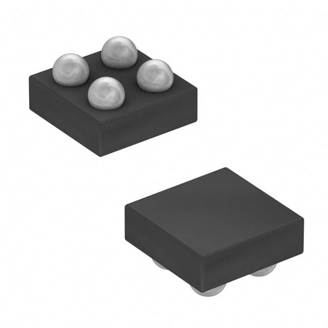
WCSP4 package: 4-bump, 2×2 array, 0.4 mm pitch, 0.8 mm × 0.8 mm body, 0.5 mm height, SAC396 bumps, backside laser marking. Coplanarity ≤0.05 mm.

Pin/Terminal Circuit Role Design Meaning
A1 IN n-Channel MOSFET drain - connects to input power rail; requires local 4.7 μF ceramic bypass capacitor placed adjacent to pin.
A2 OUT n-Channel MOSFET source - delivers switched output; requires 0.1 μF ceramic decoupling to GND for controlled slew rate.
B1 EN Active-high enable input with internal pull-down - asserts logic high ≥1.5 V to turn on; ≤0.1 V to fully disable; no external resistor needed.
B2 GND Power ground reference - must be connected to system ground plane with low-inductance path; serves as MOSFET source return and charge-pump reference.

Key Features

Feature Design Value
Guaranteed Turn-off Delay ≥30 μs (90 μs typical) - enables precise timing control for sequenced power-down of downstream ICs without external RC networks.
Low-Voltage Logic Compatibility VIL ≤ 0.1 V, VIH ≥ 1.5 V - eliminates need for level shifters when driven by sub-1 V I/O standards (e.g., LPDDR4, MIPI D-PHY).
Reverse Current Blocking IRB ≤ 10 nA - prevents cross-rail leakage in multi-supply systems where VOUT may exceed VIN during sleep or fault conditions.
Integrated EN Pull-down Ensures default OFF state at power-up - removes requirement for external pull-down resistor, saving board space and BOM count.
Thermally Optimized WCSP4 θJA = 280 °C/W - supports 1.2 A continuous operation up to +70 °C ambient when mounted per Vishay land pattern with full thermal pad soldering.

Applications

Smartphone Power Sequencing Portable Medical Sensor Hub

Use Scenario: Controlled power-up/down of camera module, NFC transceiver, or GPS receiver in response to AP commands.

IC Role / Device Role / Timing Role: High-side load switch providing isolated 1.2 V or 1.8 V rail with guaranteed 90 μs turn-off delay to meet SoC reset timing requirements.

Use Value: Eliminates need for discrete RC timing networks while ensuring compliance with JEDEC JESD78 latch-up immunity during rail transitions.

Use Scenario: Enabling/disabling ECG front-end analog signal chain during patient measurement cycles to minimize battery drain.

IC Role / Device Role / Timing Role: Low-quiescent-current (≤60 μA) load switch with reverse blocking, isolating sensitive analog circuitry from noisy digital domains.

Use Value: Prevents backfeed-induced offset drift in instrumentation amplifiers when auxiliary rails remain active during sensor sleep mode.

Industrial Handheld Terminal Wearable Fitness Tracker

Use Scenario: Power gating of Bluetooth LE radio and display driver ICs between scan intervals in ruggedized field devices.

IC Role / Device Role / Timing Role: High-reliability load switch rated for -40 °C to +85 °C operation, with 55 mΩ RDS(on) minimizing voltage drop across long flex-cable interconnects.

Use Value: Maintains ≥1.15 V at 1.2 A load over temperature, ensuring stable RF transmission even at end-of-battery life (0.9 V input).

Use Scenario: Dynamic power management of optical heart-rate sensor and accelerometer during motion-sensing duty cycles.

IC Role / Device Role / Timing Role: Ultra-small WCSP4 footprint load switch enabling <10 mm² total solution size for coin-cell-powered wearables.

Use Value: 0.8 mm × 0.8 mm package reduces PCB area by >60% vs. comparable SOT-563 solutions, preserving space for larger battery cells.

Equivalent & Alternatives

The following parts are listed as comparable options for similar high-side load switch applications.

Alternative Part Technical Difference Application Difference Selection Advice
SiP32452DB-T2-GE1 Identical package, RDS(on), and voltage range; turn-off delay <1 μs (vs. ≥30 μs), no output discharge. Suitable for fast-switching applications requiring immediate rail collapse (e.g., CPU core domain gating), not for sequenced shutdown. Select SiP32452DB-T2-GE1 only if deterministic slow turn-off is unnecessary and faster deactivation is required.
TCK107AG,LF 0.5 V–5.5 V range, 45 mΩ RDS(on), 1.5 A rating, SC-88 package (2.0 mm × 2.1 mm); no guaranteed turn-off delay spec. Larger footprint, wider voltage support, but lacks SIP32453DB-T2-GE1's timing guarantee and ultra-low-VIN capability. Choose TCK107AG,LF when operating above 2.5 V or needing higher current, accepting trade-offs in size and timing precision.

Compared with SiP32452DB-T2-GE1 and TCK107AG,LF, SIP32453DB-T2-GE1 uniquely delivers guaranteed ≥30 μs turn-off delay within a 0.8 mm × 0.8 mm WCSP4 package and sub-1 V operation - making it irreplaceable for battery-powered systems requiring controlled, repeatable power-rail decay timing without added passive components.

Availability

SIP32453DB-T2-GE1 is available at Aetrix Electronics and suitable for smartphone power sequencing, portable medical sensor hubs, industrial handheld terminals, wearable fitness trackers, and battery-backed real-time clock modules requiring stable component supply across extended production lifecycles.

Supply support for SIP32453DB-T2-GE1 includes scheduled delivery planning, volume procurement assistance, BOM continuity management, traceable sourcing, and lifecycle availability coordination for OEM customers, industrial embedded developers, connected-device designers, and electronics production programs.

Manufacturer

Vishay Siliconix designs and manufactures high-performance analog and discrete semiconductors, specializing in power management, MOSFETs, and load switches for demanding portable and industrial applications.

The SiP3245x family was developed specifically for ultra-low-voltage, space-constrained battery-operated devices requiring precise power rail control, fast turn-on, and deterministic turn-off timing - with SIP32453DB-T2-GE1 targeting applications needing guaranteed slow turn-off behavior.

FAQ

What is the guaranteed turn-off delay specification for SIP32453DB-T2-GE1?

The SIP32453DB-T2-GE1 guarantees a minimum turn-off delay of 30 μs, with a typical value of 90 μs at VIN = 1.2 V and 86 μs at VIN = 2.5 V. This parameter is explicitly specified in the datasheet's "Output turn-off delay time" table and distinguishes SIP32453DB-T2-GE1 from SiP32451/SiP32452, which have <1 μs turn-off delay. The guaranteed minimum ensures predictable power-down timing in safety-critical sequences.

Does SIP32453DB-T2-GE1 include an output discharge function?

No, SIP32453DB-T2-GE1 does not include an output discharge circuit. That feature is exclusive to SiP32451DB-T2-GE1, as confirmed in the Product Summary table and "FEATURES" section of the datasheet. SIP32453DB-T2-GE1 retains reverse current blocking and guaranteed turn-off delay but omits the internal discharge FET and associated pull-down resistance (RPD), simplifying its internal structure for timing-critical use cases.

What is the maximum continuous current rating for SIP32453DB-T2-GE1, and how is it limited?

The SIP32453DB-T2-GE1 has a maximum continuous switch current rating of 1.2 A, as defined in the Absolute Maximum Ratings table. This limit is governed by both package thermal dissipation (PD = 196 mW at TA = 70 °C, θJA = 280 °C/W) and RDS(on) temperature coefficient (3900 ppm/°C). Exceeding 1.2 A risks junction temperature exceeding 125 °C, even if RDS(on) alone would permit higher current - hence the 1.2 A rating is conservative and thermally enforced.

Is SIP32453DB-T2-GE1 compatible with 0.8 V GPIO control signals?

No, SIP32453DB-T2-GE1 is not guaranteed to operate reliably with 0.8 V GPIO signals. Its EN input low voltage (VIL) is specified as ≤0.1 V max at VIN = 1 V, and its EN input high voltage (VIH) is ≥1.5 V min at VIN = 2.5 V. A 0.8 V logic high falls below the required VIH threshold and may result in incomplete turn-on or increased RDS(on); verified operation begins at ≥1.5 V logic high.

What package type and dimensions does SIP32453DB-T2-GE1 use?

SIP32453DB-T2-GE1 uses the WCSP4 (Wafer-Level Chip-Scale Package) with 4 bumps in a 2×2 array, 0.4 mm pitch, 0.8 mm × 0.8 mm body size, and 0.5 mm height. Per Vishay DWG-No: 6004, recommended land pattern uses 0.15–0.20 mm diameter solder pads with solder mask opening equal to pad diameter plus 0.1 mm - critical for achieving full thermal and electrical performance.

SIP32453DB-T2-GE1 Specifications

Product attributes
Attribute value
Manufacturer:
Vishay Siliconix
Package/Case:
4-UFBGA, CSPBGA
Series:
MICRO FOOT®
Packaging:
Tape & Reel (TR)
Product Status:
Active
Switch Type:
General Purpose
Number of Outputs:
1
Ratio - Input:Output:
1:1
Output Configuration:
High Side
Output Type:
N-Channel
Interface:
On/Off
Voltage - Load:
0.9V ~ 2.5V
Voltage - Supply (Vcc/Vdd):
Not Required
Current - Output (Max):
1.2A
Rds On (Typ):
54mOhm
Input Type:
Non-Inverting
Features:
-
Fault Protection:
Reverse Current
Operating Temperature:
-40°C ~ 125°C (TJ)
Grade:
-
Qualification:
-
Mounting Type:
Surface Mount
Supplier Device Package:
4-WCSP (0.76x0.76)

SIP32453DB-T2-GE1 FAQ

1.How can I place an order for SIP32453DB-T2-GE1 through Aetrix?

Please submit a Request for Quotation (RFQ) for SIP32453DB-T2-GE1 on Aetrix. Our sales agent will provide a competitive quotation and guide you through the order confirmation once you accept the terms.

2.Are the price and stock information for SIP32453DB-T2-GE1 reliable?

The price and inventory of SIP32453DB-T2-GE1 are updated periodically and may fluctuate due to market conditions. Stock and pricing data are typically refreshed every 24 hours. Quotation validity for SIP32453DB-T2-GE1 is usually 5 days.

3.What payment methods are accepted for SIP32453DB-T2-GE1?

We accept Wire Transfer, PayPal, Credit Card, Western Union, MoneyGram, and Escrow for SIP32453DB-T2-GE1 transactions.

Note: Certain payment methods may incur a processing fee.

4.How is shipping managed for SIP32453DB-T2-GE1?

SIP32453DB-T2-GE1 orders can be shipped via leading logistics carriers, including DHL, UPS, FedEx, TNT, or Registered Mail.

Once your SIP32453DB-T2-GE1 order is processed, you will receive an email with the shipment details and tracking number.

Note: Tracking information may take up to 24 hours to appear. Express delivery typically takes 3–5 business days.

5.How can I obtain technical support or documentation for SIP32453DB-T2-GE1?

For technical support, including SIP32453DB-T2-GE1 datasheets, pinout diagrams, or application guidance, please contact our engineering support team. They can provide detailed documentation and assistance for your SIP32453DB-T2-GE1 requirements.

6.How does Aetrix verify that SIP32453DB-T2-GE1 is sourced from the original manufacturer or authorized distributors?

All SIP32453DB-T2-GE1 products on Aetrix are procured from qualified distributors and authorized channels. Our dedicated quality assurance team conducts strict verification, including traceability checks and, if necessary, third-party testing. This ensures that SIP32453DB-T2-GE1 meets industry standards.

7.What is the process for return or replacement of SIP32453DB-T2-GE1?

All SIP32453DB-T2-GE1 units undergo pre-shipment inspection (PSI). If there is an issue with SIP32453DB-T2-GE1, returns or replacements are accepted under the following conditions:

1.Quantity discrepancies, incorrect items, or visible external defects (such as breakage or corrosion), acknowledged by Aetrix.

2.The issue is reported within 90 days of delivery.

3.The SIP32453DB-T2-GE1 part is unused and in its original packaging.

Return procedure for SIP32453DB-T2-GE1:

1.Submit a request within 90 days.

2.Obtain a Return Material Authorization (RMA) from Aetrix.

SIP32453DB-T2-GE1 Tags

  • SIP32453DB-T2-GE1
  • SIP32453DB-T2-GE1 PDF
  • SIP32453DB-T2-GE1 Datasheet
  • SIP32453DB-T2-GE1 Specifications
  • SIP32453DB-T2-GE1 Images
  • Vishay Siliconix
  • Vishay Siliconix SIP32453DB-T2-GE1
  • Buy SIP32453DB-T2-GE1
  • SIP32453DB-T2-GE1 Price
  • SIP32453DB-T2-GE1 Distributor
  • SIP32453DB-T2-GE1 Supplier
  • SIP32453DB-T2-GE1 Wholesale
Related Products
TPS22919DCKR
TPS22919DCKR

Texas Instruments

MIC2091-1YM5-TR
MIC2091-1YM5-TR

Microchip Technology

MIC2090-1YM5-TR
MIC2090-1YM5-TR

Microchip Technology

TPS22995RZFR
TPS22995RZFR

Texas Instruments

TPS22975DSGR
TPS22975DSGR

Texas Instruments

SIP32510DT-T1-GE3
SIP32510DT-T1-GE3

Vishay Siliconix

ULN2003D1013TR
ULN2003D1013TR

STMicroelectronics

MIC2005A-1YM5-TR
MIC2005A-1YM5-TR

Microchip Technology

MIC2005A-1YM6-TR
MIC2005A-1YM6-TR

Microchip Technology

TPS22916BYFPR
TPS22916BYFPR

Texas Instruments

TPS22917DBVR
TPS22917DBVR

Texas Instruments

ULN2003APWR
ULN2003APWR

Texas Instruments

Tech Hub

Search

Search

PRODUCT

PRODUCT

PHONE

PHONE

USER

USER