Send an Inquiry

To receive a quote for your project, please fill in the following information, and we’ll get back to you promptly.

Name*
Company*
Email Address*
Phone/WhatsApp
Part Number*
Quantity*
Message
Submit Inventory List

Please fill in the following information, and we’ll get back to you promptly.

Name*
Company*
Email Address*
Phone/WhatsApp
Upload My List
Message

Vishay Siliconix SIP32468DB-T2-GE1

Part No.:
SIP32468DB-T2-GE1
Manufacturer:
Vishay Siliconix
Category:
Power Distribution Switches, Load Drivers
Package:
4-UFBGA, WLCSP
Datasheet:
AetrixSIP32468DB-T2-GE1.pdf
Description:
IC PWR SWITCH N-CHAN 1:1 4WLCSP
Quantity:
Payment:
Payment
Shipping:
Shipping

Inventory:3,334

Please send an inquiry. Send us your inquiry, and we will respond immediately.

Part Number
Quantity*
Price
Name*
Company
Email*
Comments

Product details

Overview

SIP32468DB-T2-GE1 from Vishay Siliconix is a slew-rate-controlled, high-side load switch IC operating from 1.2 V to 5.5 V input voltage, featuring 54 mΩ typical RDS(on) at 3 V, integrated output discharge, reverse current blocking, and logic-low enable. It serves as a power-path control device in portable battery-powered systems requiring controlled inrush current and automatic output discharge during shutdown.

For engineers reviewing the SIP32468DB-T2-GE1 datasheet, SIP32468DB-T2-GE1 pinout, SIP32468DB-T2-GE1 application, or SIP32468DB-T2-GE1 equivalent, key selection criteria include its 300 μs slew-controlled turn-on time, WCSP4 0.76 mm × 0.76 mm package with 0.4 mm pitch, integrated EN pull-up resistor (2.6 MΩ), and guaranteed reverse blocking up to 5 V output when disabled.

Technical Context

The SIP32468DB-T2-GE1 integrates a negative charge pump to maintain high gate-to-source voltage across low input voltages (1.2 V–5.5 V), enabling stable low RDS(on) performance. Its internal slew-rate control circuit limits dV/dt at the output to suppress inrush current during turn-on.

Unlike the SiP32467 variant, SIP32468DB-T2-GE1 includes an integrated output discharge switch (RPD < 200 Ω at 1.8 V) that actively pulls VOUT to GND when EN is deasserted. It also features reverse current blocking (IIN(RB) ≤ 1 nA at VOUT = 5 V, VIN = 0 V) and a built-in 2.6 MΩ pull-up resistor from EN to IN.

Key Specifications

ParameterValue and Actual Design Meaning
Input Voltage Range1.2 V to 5.5 V - supports single-cell Li-ion, Li-polymer, and multi-rail PMIC outputs without level-shifting.
RDS(on) (typ. @ 3 V)54 mΩ - enables ≤ 1.2 A continuous switching with ≤ 65 mW conduction loss at full load.
Slew Rate Control300 μs rise time - limits inrush current to protect upstream power sources and downstream capacitors.
Output DischargeIntegrated pulldown (RPD < 200 Ω @ 1.8 V) - discharges VOUT within milliseconds after disable, preventing floating or latch-up in downstream circuits.
Reverse Blocking Current≤ 1 nA @ VOUT = 5 V, VIN = 0 V - prevents backflow from higher-voltage rails (e.g., USB OTG, auxiliary supplies) into main battery path.
EN Logic PolarityActive-low with internal 2.6 MΩ pull-up - simplifies interface to 1.2 V–3.3 V GPIOs; no external pull-up required.
Quiescent Current6 μA @ VIN = 3.3 V - minimizes standby power draw in always-on subsystems (e.g., RTC, sensors).

Pinout & Package

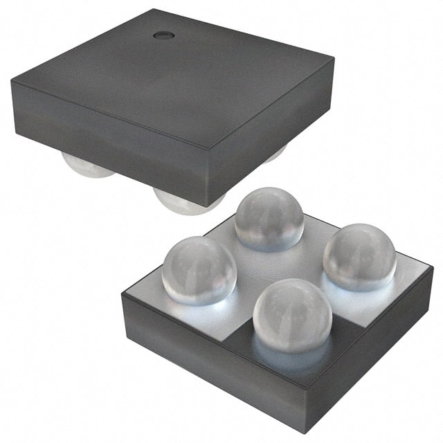
Package: WCSP4 (Wafer-Level Chip-Scale Package), 2 × 2 bump array, 0.76 mm × 0.76 mm footprint, 0.4 mm pitch, 0.5 mm height, solder bumps SAC396.

Pin/TerminalCircuit RoleDesign Meaning
A1OUTSwitch output node - connects to load capacitance and downstream circuitry; internally discharged when EN = high.
A2INPower input - accepts 1.2 V–5.5 V supply; source for internal charge pump and EN pull-up resistor.
B1GNDGround reference - must be low-impedance connection to system ground plane for thermal and noise integrity.
B2ENEnable control - logic-low turns switch ON; internal 2.6 MΩ pull-up to IN ensures default OFF state if left floating.

Key Features

FeatureDesign Value
Integrated Output DischargeEnables fast, deterministic VOUT discharge (< 1 ms for 10 μF load) without external FET or resistor network.
Reverse Current BlockingPrevents backfeed from higher-voltage outputs (e.g., USB VBUS) into battery rail, eliminating need for external diode or ideal diode controller.
Slew-Rate Controlled Turn-OnGuarantees 300 μs output rise time - eliminates voltage droop on shared input rails and avoids false resets in sensitive digital loads.
Low-Voltage CompatibilityOperates down to 1.2 V input - supports modern ultra-low-power SoCs and sub-1.8 V I/O domains without external biasing.
WCSP4 Miniaturization0.76 mm × 0.76 mm footprint - saves >70% board area vs. comparable SOT-23 or DFN packages, critical for space-constrained mobile designs.

Applications

Smartphone Power ManagementPortable Medical Sensor Hub

Use Scenario: Isolating camera module or NFC transceiver from main battery during sleep mode while retaining fast wake-up capability.

IC Role / Device Role / Timing Role: High-side load switch controlling power delivery to peripheral subsystems; slew-controlled turn-on prevents brownout during camera activation.

Use Value: Integrated output discharge ensures NFC antenna bias settles cleanly before RF handshake; reverse blocking prevents interference from USB-C VBUS during charging.

Use Scenario: Enabling/disabling ECG front-end analog signal chain powered from low-noise LDO, with strict requirement for zero residual voltage on analog inputs during off-state.

IC Role / Device Role / Timing Role: Precision power gate with sub-nA leakage and active VOUT discharge - maintains analog input nodes at GND potential during standby.

Use Value: Eliminates need for external discharge FET and timing RC network; 1 nA reverse blocking preserves battery life over multi-week wearable deployments.

Tablet USB-C Accessory PortIndustrial Handheld Scanner

Use Scenario: Managing power to USB-C alternate mode (DisplayPort) circuitry where VOUT may exceed VIN during hot-plug events.

IC Role / Device Role / Timing Role: Bidirectional isolation switch with reverse blocking - blocks current flow from DP AUX/HPD lines back into main SoC rail when port is inactive.

Use Value: Prevents unintended power injection into SoC I/O pins; 5.5 V absolute max rating accommodates transient overshoot on USB-C CC lines.

Use Scenario: Sequencing power to laser driver and image sensor in barcode scanner, requiring synchronized discharge of both rails upon button-release shutdown.

IC Role / Device Role / Timing Role: Dual-rail enable/discharge controller - one SIP32468DB-T2-GE1 per rail provides independent slew control and discharge timing.

Use Value: 300 μs slew rate matches mechanical switch debounce window; integrated discharge eliminates risk of residual charge causing false trigger on next scan cycle.

Equivalent & Alternatives

The following parts are listed as comparable options for similar high-side load switch applications.

Alternative PartTechnical DifferenceApplication DifferenceSelection Advice
TPL7407LDRNo integrated output discharge; 7-channel NMOS array with 1.5 Ω RDS(on); requires external pull-down for discharge.Higher RDS(on) and no slew control - unsuitable for low-voltage, high-current, or inrush-sensitive loads.Select only when multi-channel discrete gating is needed and discharge is handled externally.
TPS22915BYFPR0.57 mΩ RDS(on) at 5 V but no output discharge; 0.65 mm × 0.65 mm DSBGA package; 1.6 V–5.5 V range.Lacks reverse blocking below 1.6 V input - cannot support 1.2 V SoC rails or bidirectional isolation at lowest voltages.Choose for ultra-low-loss 3.3 V/5 V rails where discharge is managed by system-level sequencing.

Compared with TPL7407LDR and TPS22915BYFPR, SIP32468DB-T2-GE1 uniquely combines sub-100 mΩ RDS(on) down to 1.2 V, integrated discharge, and guaranteed reverse blocking - making it the only option for compact, battery-critical designs requiring full rail control at minimum voltage.

Availability

SIP32468DB-T2-GE1 is available at Aetrix Electronics and suitable for smartphone power management, portable medical sensor hubs, tablet USB-C accessory ports, and industrial handheld scanners requiring stable component supply, long-term lifecycle assurance, and wafer-level packaging consistency.

Supply support for SIP32468DB-T2-GE1 includes scheduled delivery planning, volume procurement assistance, BOM continuity management, traceable sourcing, and lifecycle availability coordination for OEM customers, industrial embedded developers, connected-device designers, and electronics production programs.

Manufacturer

Vishay Siliconix is a global leader in discrete semiconductors and passive components, specializing in power MOSFETs, diodes, optoelectronics, and precision resistive solutions.

The SiP3246x family was designed specifically for space-constrained, battery-powered consumer and medical devices requiring robust power-path control with minimal external components and guaranteed low-leakage isolation.

FAQ

What is the maximum continuous current rating for SIP32468DB-T2-GE1?

The SIP32468DB-T2-GE1 has a maximum continuous switch current rating of 1.2 A, as specified in the Absolute Maximum Ratings table. This limit is thermally derived - at 70 °C ambient, power dissipation is capped at ~268 mW due to θJ-A = 205 °C/W and TJ(max) = 125 °C. Exceeding 1.2 A risks junction overheating even if RDS(on) suggests higher theoretical current capability.

Does SIP32468DB-T2-GE1 support bidirectional operation?

The SIP32468DB-T2-GE1 supports bidirectional voltage blocking (reverse current blocking) when disabled, but is not a true bidirectional switch during conduction. Its internal architecture is optimized for high-side switching from IN to OUT. While it can tolerate VOUT > VIN when off, forward conduction is unidirectional - current flows only from IN to OUT when enabled.

How does the integrated output discharge function in SIP32468DB-T2-GE1?

In SIP32468DB-T2-GE1, the integrated output discharge activates automatically when EN is driven high (device disabled). A dedicated internal NMOS switch connects OUT to GND with RPD < 200 Ω at 1.8 V, discharging typical 1–10 μF load capacitances in under 1 ms. This eliminates floating outputs and prevents unintended wake-up or latch-up in downstream circuitry.

What is the purpose of the 2.6 MΩ pull-up resistor on the EN pin of SIP32468DB-T2-GE1?

The 2.6 MΩ internal pull-up resistor on the EN pin of SIP32468DB-T2-GE1 ensures a defined logic-high state (disable condition) when the control line is left unconnected or driven high-impedance. It eliminates the need for an external pull-up and guarantees safe default-OFF behavior - critical for battery safety in portable systems where accidental power-on must be prevented.

Can SIP32468DB-T2-GE1 operate reliably at 1.2 V input voltage?

Yes, SIP32468DB-T2-GE1 is fully specified for operation at 1.2 V input voltage, with RDS(on) = 95 mΩ (max) and functional slew-rate control maintained. Its internal charge pump architecture sustains sufficient gate drive at this minimum voltage, enabling use with ultra-low-power microcontrollers and sub-1.8 V I/O domains without external level-shifting or boosting.

SIP32468DB-T2-GE1 Specifications

Product attributes
Attribute value
Manufacturer:
Vishay Siliconix
Package/Case:
4-UFBGA, WLCSP
Series:
-
Packaging:
Tape & Reel (TR)
Product Status:
Active
Switch Type:
General Purpose
Number of Outputs:
1
Ratio - Input:Output:
1:1
Output Configuration:
High Side
Output Type:
N-Channel
Interface:
On/Off
Voltage - Load:
1.2V ~ 5.5V
Voltage - Supply (Vcc/Vdd):
Not Required
Current - Output (Max):
1.2A
Rds On (Typ):
50mOhm
Input Type:
Non-Inverting
Features:
Load Discharge, Slew Rate Controlled
Fault Protection:
Reverse Current
Operating Temperature:
-40°C ~ 125°C (TJ)
Grade:
-
Qualification:
-
Mounting Type:
Surface Mount
Supplier Device Package:
4-WLCSP (0.76x0.76)

SIP32468DB-T2-GE1 FAQ

1.How can I place an order for SIP32468DB-T2-GE1 through Aetrix?

Please submit a Request for Quotation (RFQ) for SIP32468DB-T2-GE1 on Aetrix. Our sales agent will provide a competitive quotation and guide you through the order confirmation once you accept the terms.

2.Are the price and stock information for SIP32468DB-T2-GE1 reliable?

The price and inventory of SIP32468DB-T2-GE1 are updated periodically and may fluctuate due to market conditions. Stock and pricing data are typically refreshed every 24 hours. Quotation validity for SIP32468DB-T2-GE1 is usually 5 days.

3.What payment methods are accepted for SIP32468DB-T2-GE1?

We accept Wire Transfer, PayPal, Credit Card, Western Union, MoneyGram, and Escrow for SIP32468DB-T2-GE1 transactions.

Note: Certain payment methods may incur a processing fee.

4.How is shipping managed for SIP32468DB-T2-GE1?

SIP32468DB-T2-GE1 orders can be shipped via leading logistics carriers, including DHL, UPS, FedEx, TNT, or Registered Mail.

Once your SIP32468DB-T2-GE1 order is processed, you will receive an email with the shipment details and tracking number.

Note: Tracking information may take up to 24 hours to appear. Express delivery typically takes 3–5 business days.

5.How can I obtain technical support or documentation for SIP32468DB-T2-GE1?

For technical support, including SIP32468DB-T2-GE1 datasheets, pinout diagrams, or application guidance, please contact our engineering support team. They can provide detailed documentation and assistance for your SIP32468DB-T2-GE1 requirements.

6.How does Aetrix verify that SIP32468DB-T2-GE1 is sourced from the original manufacturer or authorized distributors?

All SIP32468DB-T2-GE1 products on Aetrix are procured from qualified distributors and authorized channels. Our dedicated quality assurance team conducts strict verification, including traceability checks and, if necessary, third-party testing. This ensures that SIP32468DB-T2-GE1 meets industry standards.

7.What is the process for return or replacement of SIP32468DB-T2-GE1?

All SIP32468DB-T2-GE1 units undergo pre-shipment inspection (PSI). If there is an issue with SIP32468DB-T2-GE1, returns or replacements are accepted under the following conditions:

1.Quantity discrepancies, incorrect items, or visible external defects (such as breakage or corrosion), acknowledged by Aetrix.

2.The issue is reported within 90 days of delivery.

3.The SIP32468DB-T2-GE1 part is unused and in its original packaging.

Return procedure for SIP32468DB-T2-GE1:

1.Submit a request within 90 days.

2.Obtain a Return Material Authorization (RMA) from Aetrix.

SIP32468DB-T2-GE1 Tags

  • SIP32468DB-T2-GE1
  • SIP32468DB-T2-GE1 PDF
  • SIP32468DB-T2-GE1 Datasheet
  • SIP32468DB-T2-GE1 Specifications
  • SIP32468DB-T2-GE1 Images
  • Vishay Siliconix
  • Vishay Siliconix SIP32468DB-T2-GE1
  • Buy SIP32468DB-T2-GE1
  • SIP32468DB-T2-GE1 Price
  • SIP32468DB-T2-GE1 Distributor
  • SIP32468DB-T2-GE1 Supplier
  • SIP32468DB-T2-GE1 Wholesale
Related Products
TPS22919DCKR
TPS22919DCKR

Texas Instruments

MIC2091-1YM5-TR
MIC2091-1YM5-TR

Microchip Technology

MIC2090-1YM5-TR
MIC2090-1YM5-TR

Microchip Technology

TPS22995RZFR
TPS22995RZFR

Texas Instruments

TPS22975DSGR
TPS22975DSGR

Texas Instruments

SIP32510DT-T1-GE3
SIP32510DT-T1-GE3

Vishay Siliconix

ULN2003D1013TR
ULN2003D1013TR

STMicroelectronics

MIC2005A-1YM5-TR
MIC2005A-1YM5-TR

Microchip Technology

MIC2005A-1YM6-TR
MIC2005A-1YM6-TR

Microchip Technology

TPS22916BYFPR
TPS22916BYFPR

Texas Instruments

TPS22917DBVR
TPS22917DBVR

Texas Instruments

ULN2003APWR
ULN2003APWR

Texas Instruments

Tech Hub

Search

Search

PRODUCT

PRODUCT

PHONE

PHONE

USER

USER