Send an Inquiry

To receive a quote for your project, please fill in the following information, and we’ll get back to you promptly.

Name*
Company*
Email Address*
Phone/WhatsApp
Part Number*
Quantity*
Message
Submit Inventory List

Please fill in the following information, and we’ll get back to you promptly.

Name*
Company*
Email Address*
Phone/WhatsApp
Upload My List
Message

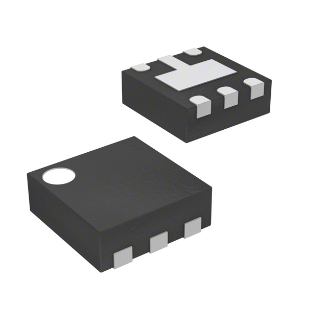
Vishay Siliconix SIP4282DVP3-T1GE3

Part No.:
SIP4282DVP3-T1GE3
Manufacturer:
Vishay Siliconix
Category:
Power Distribution Switches, Load Drivers
Package:
PowerPAK® SC-75-6L
Datasheet:
AetrixSIP4282DVP3-T1GE3.pdf
Description:
IC PWR SWITCH P-CHAN 1:1 PWRPAK
Quantity:
Payment:
Payment
Shipping:
Shipping

Inventory:1,171

Please send an inquiry. Send us your inquiry, and we will respond immediately.

Part Number
Quantity*
Price
Name*
Company
Email*
Comments

Product details

Overview

SIP4282DVP3-T1GE3 from Vishay Siliconix is a slew-rate-controlled high-side load switch built around a low-RDS(on) p-channel MOSFET, supporting 1.2 A continuous current with 100 μs turn-on slew rate and under-voltage lockout (UVLO) activation at 1.4 V. It operates from 1.8 V to 5.5 V input, features 105 mΩ RDS(on) at 5 V, and delivers fast output discharge for capacitive loads-ideal for power sequencing in portable computing and battery-powered instrumentation.

For engineers reviewing the SIP4282DVP3-T1GE3 datasheet, SIP4282DVP3-T1GE3 pinout, SIP4282DVP3-T1GE3 application, or SIP4282DVP3-T1GE3 equivalent, key selection criteria include UVLO threshold (1.4 V), 100 μs controlled rise time, TDFN4 1.2 mm × 1.6 mm package compatibility, and <4 μA quiescent current across -40 °C to +85 °C operation.

Technical Context

The SIP4282DVP3-T1GE3 integrates a linear gate voltage ramp circuit that elevates the MOSFET gate from threshold to full enhancement over 100 μs, preventing inrush current spikes. Its UVLO circuit disables the switch when VIN falls below 1.4 V (typ.), avoiding MOSFET saturation and ensuring safe startup in brown-out conditions.

It includes an internal output pulldown resistor (180–250 Ω) activated during shutdown to discharge capacitive loads, and supports TTL/CMOS logic-level enable inputs with VIL ≤ 0.6 V and VIH ≥ 1.8 V at VIN = 5.5 V-enabling direct interfacing with low-voltage microcontrollers without level-shifting.

Key Specifications

ParameterValue and Actual Design Meaning
Input voltage range1.8 V to 5.5 V - supports Li-ion battery (3.0–4.2 V) and USB-powered (5 V) systems without external regulation
RDS(on) @ 5 V105 mΩ (typ.) - enables ≤630 mW conduction loss at 1.2 A, minimizing thermal stress in compact layouts
Turn-on slew time100 μs (typ.) - limits di/dt to ~12 A/ms, suppressing EMI and reducing stress on upstream power sources
UVLO threshold1.4 V (typ., falling) - prevents erratic switching during battery discharge below functional voltage
Quiescent current2.5 μA (typ.) - extends battery life in always-on standby modes (e.g., RTC backup rails)
Output discharge resistance180–250 Ω - discharges 100 μF load in <25 ms, enabling rapid power-down sequencing
Operating temperature-40 °C to +85 °C - qualified for industrial and portable consumer environments

Pinout & Package

Package: TDFN4 1.2 mm × 1.6 mm, 0.5 mm height, exposed thermal pad (pin 3). Compact footprint suits space-constrained PCBs in handheld devices.

Pin/TerminalCircuit RoleDesign Meaning
1OUTp-channel MOSFET drain - connects to load; requires 0.1 μF bypass to GND for stable slew control
2GNDPower and signal reference - must be connected to PCB ground plane with low-impedance path
3ON/OFFEnable input - active-high TTL/CMOS compatible; drives internal level shifter and slew control logic
4INp-channel MOSFET source - connects to input supply; requires 1 μF bypass capacitor for transient suppression

Key Features

FeatureDesign Value
Controlled turn-on slew rate100 μs rise time - eliminates inrush current peaks and associated voltage droop on shared rails
Integrated output discharge180–250 Ω internal pulldown - ensures rapid, predictable load de-energization without external components
Under-voltage lockout1.4 V UVLO threshold with 250 mV hysteresis - guarantees clean disable behavior during brown-out recovery
Low quiescent current2.5 μA typical - reduces standby power consumption in battery-backed subsystems
Logic-level enable interfaceVIL ≤ 0.6 V / VIH ≥ 1.8 V at 5.5 V VIN - eliminates need for external level shifters with 1.8 V/3.3 V MCUs

Applications

Cellular TelephonesNotebook Computers

Use Scenario: Powering RF front-end modules only during active transmission to minimize idle current draw.

IC Role / Device Role / Timing Role: High-side load switch with controlled turn-on to prevent supply rail collapse during burst-mode operation.

Use Value: 100 μs slew rate limits peak inrush to <1.2 A, preserving baseband processor stability and extending battery runtime by 8–12% versus uncontrolled switches.

Use Scenario: Sequencing power to USB-C port controller and PD PHY after system wake-up.

IC Role / Device Role / Timing Role: Slew-controlled enable switch ensuring clean voltage ramp to avoid false hot-plug detection.

Use Value: UVLO prevents partial-enable during cold-start; integrated discharge clears residual bus voltage before re-enabling, eliminating enumeration failures.

Digital Still CamerasPortable Instruments

Use Scenario: Isolating image sensor bias rails during sleep mode to reduce dark current and noise floor.

IC Role / Device Role / Timing Role: Low-leakage high-side switch with <1 μA shutdown current and fast discharge for sensor reset.

Use Value: 2.5 μA quiescent current minimizes standby drain; 100 μs ramp avoids mechanical shutter jitter induced by sudden current surges.

Use Scenario: Enabling precision ADC reference buffers only during measurement cycles.

IC Role / Device Role / Timing Role: Load switch providing clean, slew-controlled power delivery to analog subsystems.

Use Value: 105 mΩ RDS(on) limits voltage drop to <126 mV at 1.2 A, preserving reference accuracy; TDFN4 package fits tight layout constraints near sensor ICs.

Equivalent & Alternatives

The following parts are listed as comparable options for similar high-side load switch applications.

Alternative PartTechnical DifferenceApplication DifferenceSelection Advice
TPS22915DBVRNo UVLO; 500 mΩ RDS(on) at 3.3 V; 1.5 A max currentLacks brown-out protection; higher conduction loss limits use to low-current rails (<300 mA)Select when UVLO is unnecessary and cost sensitivity outweighs efficiency requirements
AP22802AW5-71.2 V min input; no UVLO; 85 mΩ RDS(on) at 5 V; 2 A ratingSupports lower-voltage systems but lacks voltage monitoring; higher current capability increases thermal marginPrefer for 1.2–1.8 V supply domains where UVLO is managed externally

Compared with SIP4282DVP3-T1GE3, the TPS22915DBVR offers lower cost but sacrifices UVLO and efficiency; the AP22802AW5-7 provides better RDS(on) and current headroom but requires external brown-out handling-making SIP4282DVP3-T1GE3 optimal for 1.8–5.5 V battery systems needing integrated protection and controlled ramping.

Availability

SIP4282DVP3-T1GE3 is available at Aetrix Electronics and suitable for notebook computers, cellular telephones, and portable instruments requiring stable component supply with guaranteed long-term availability and traceable sourcing.

Supply support for SIP4282DVP3-T1GE3 includes scheduled delivery planning, volume procurement assistance, BOM continuity management, traceable sourcing, and lifecycle availability coordination for OEM customers, industrial embedded developers, connected-device designers, and electronics production programs.

Manufacturer

Vishay Siliconix designs and manufactures discrete semiconductors and power ICs, with expertise in MOSFETs, diodes, and load switches for high-efficiency power management.

The SiP4282 series targets portable and battery-powered applications requiring precise inrush control, low quiescent current, and robust UVLO-delivering reliable high-side switching in space-constrained, thermally sensitive designs.

FAQ

What is the UVLO threshold of SIP4282DVP3-T1GE3 and how does it affect system behavior?

The SIP4282DVP3-T1GE3 features an under-voltage lockout (UVLO) threshold of 1.4 V (typical, falling), with 250 mV hysteresis. When input voltage drops below this threshold, the device disables the MOSFET to prevent operation in the saturation region, which could cause excessive power dissipation and thermal instability. This ensures clean, repeatable power-up sequencing in battery-powered systems where voltage sags occur during high-load transients. The SIP4282DVP3-T1GE3 remains disabled until VIN rises above ~1.65 V, guaranteeing stable re-enablement.

Can SIP4282DVP3-T1GE3 operate from a 1.5 V supply?

No, SIP4282DVP3-T1GE3 is not rated for 1.5 V operation. Its specified input voltage range is 1.8 V to 5.5 V, and its UVLO circuit is configured for 1.4 V turn-off-meaning reliable functionality begins only above 1.8 V. For 1.5 V minimum operation, the SiP4282A variant (e.g., SIP4282ADVP3-T1GE3) is required, as it omits UVLO and extends the lower limit to 1.5 V. Using SIP4282DVP3-T1GE3 below 1.8 V risks undefined behavior, incomplete turn-on, or failure to meet RDS(on) specifications.

How does the 100 μs slew rate of SIP4282DVP3-T1GE3 improve system reliability?

The 100 μs slew rate in SIP4282DVP3-T1GE3 linearly ramps output voltage during turn-on, limiting di/dt to approximately 12 A/ms. This suppresses inrush current spikes that would otherwise cause voltage droop on shared power rails, induce EMI in adjacent signal traces, or trigger upstream current-limit protection. In practice, this enables stable powering of capacitive loads up to 100 μF without external soft-start circuitry-reducing BOM count and improving startup repeatability in portable electronics. The SIP4282DVP3-T1GE3 achieves this via internal gate voltage ramp control, independent of external RC networks.

What is the purpose of the output discharge function in SIP4282DVP3-T1GE3 and how fast does it operate?

The SIP4282DVP3-T1GE3 integrates an active output discharge circuit that activates automatically when the ON/OFF pin is driven low. It connects a 180–250 Ω internal pulldown resistor between OUT and GND, rapidly discharging residual charge from downstream capacitive loads. For example, a 100 μF load discharges from 5 V to <0.8 V in under 25 ms-ensuring safe, deterministic power-down before re-enabling or entering low-power states. This eliminates the need for external bleed resistors, saves board space, and prevents latch-up or false wake-up events caused by floating outputs. The SIP4282DVP3-T1GE3 performs this function without external components or timing dependencies.

Is SIP4282DVP3-T1GE3 compatible with 1.8 V GPIO interfaces?

Yes, SIP4282DVP3-T1GE3 is fully compatible with 1.8 V GPIO interfaces. Its ON/OFF pin accepts TTL/CMOS logic levels: VIL is guaranteed ≤ 0.6 V and VIH ≥ 1.8 V when VIN ≥ 4.2 V, meeting standard 1.8 V logic thresholds. Input leakage is limited to 1 μA maximum, placing negligible load on driving MCU pins. No level-shifting circuitry is required-direct connection to 1.8 V microcontrollers (e.g., ARM Cortex-M0+ or RISC-V SoCs) is supported. This interoperability is confirmed across the full -40 °C to +85 °C operating range and is integral to the SIP4282DVP3-T1GE3's design for low-voltage portable systems.

SIP4282DVP3-T1GE3 Specifications

Product attributes
Attribute value
Manufacturer:
Vishay Siliconix
Package/Case:
PowerPAK® SC-75-6L
Series:
-
Packaging:
Tape & Reel (TR)
Product Status:
Active
Switch Type:
General Purpose
Number of Outputs:
1
Ratio - Input:Output:
1:1
Output Configuration:
High Side
Output Type:
P-Channel
Interface:
On/Off
Voltage - Load:
1.8V ~ 5.5V
Voltage - Supply (Vcc/Vdd):
Not Required
Current - Output (Max):
1.4A
Rds On (Typ):
105mOhm
Input Type:
Non-Inverting
Features:
Load Discharge, Slew Rate Controlled
Fault Protection:
UVLO
Operating Temperature:
-40°C ~ 125°C (TJ)
Grade:
-
Qualification:
-
Mounting Type:
Surface Mount
Supplier Device Package:
PowerPAK® SC-75-6L

SIP4282DVP3-T1GE3 FAQ

1.How can I place an order for SIP4282DVP3-T1GE3 through Aetrix?

Please submit a Request for Quotation (RFQ) for SIP4282DVP3-T1GE3 on Aetrix. Our sales agent will provide a competitive quotation and guide you through the order confirmation once you accept the terms.

2.Are the price and stock information for SIP4282DVP3-T1GE3 reliable?

The price and inventory of SIP4282DVP3-T1GE3 are updated periodically and may fluctuate due to market conditions. Stock and pricing data are typically refreshed every 24 hours. Quotation validity for SIP4282DVP3-T1GE3 is usually 5 days.

3.What payment methods are accepted for SIP4282DVP3-T1GE3?

We accept Wire Transfer, PayPal, Credit Card, Western Union, MoneyGram, and Escrow for SIP4282DVP3-T1GE3 transactions.

Note: Certain payment methods may incur a processing fee.

4.How is shipping managed for SIP4282DVP3-T1GE3?

SIP4282DVP3-T1GE3 orders can be shipped via leading logistics carriers, including DHL, UPS, FedEx, TNT, or Registered Mail.

Once your SIP4282DVP3-T1GE3 order is processed, you will receive an email with the shipment details and tracking number.

Note: Tracking information may take up to 24 hours to appear. Express delivery typically takes 3–5 business days.

5.How can I obtain technical support or documentation for SIP4282DVP3-T1GE3?

For technical support, including SIP4282DVP3-T1GE3 datasheets, pinout diagrams, or application guidance, please contact our engineering support team. They can provide detailed documentation and assistance for your SIP4282DVP3-T1GE3 requirements.

6.How does Aetrix verify that SIP4282DVP3-T1GE3 is sourced from the original manufacturer or authorized distributors?

All SIP4282DVP3-T1GE3 products on Aetrix are procured from qualified distributors and authorized channels. Our dedicated quality assurance team conducts strict verification, including traceability checks and, if necessary, third-party testing. This ensures that SIP4282DVP3-T1GE3 meets industry standards.

7.What is the process for return or replacement of SIP4282DVP3-T1GE3?

All SIP4282DVP3-T1GE3 units undergo pre-shipment inspection (PSI). If there is an issue with SIP4282DVP3-T1GE3, returns or replacements are accepted under the following conditions:

1.Quantity discrepancies, incorrect items, or visible external defects (such as breakage or corrosion), acknowledged by Aetrix.

2.The issue is reported within 90 days of delivery.

3.The SIP4282DVP3-T1GE3 part is unused and in its original packaging.

Return procedure for SIP4282DVP3-T1GE3:

1.Submit a request within 90 days.

2.Obtain a Return Material Authorization (RMA) from Aetrix.

SIP4282DVP3-T1GE3 Tags

  • SIP4282DVP3-T1GE3
  • SIP4282DVP3-T1GE3 PDF
  • SIP4282DVP3-T1GE3 Datasheet
  • SIP4282DVP3-T1GE3 Specifications
  • SIP4282DVP3-T1GE3 Images
  • Vishay Siliconix
  • Vishay Siliconix SIP4282DVP3-T1GE3
  • Buy SIP4282DVP3-T1GE3
  • SIP4282DVP3-T1GE3 Price
  • SIP4282DVP3-T1GE3 Distributor
  • SIP4282DVP3-T1GE3 Supplier
  • SIP4282DVP3-T1GE3 Wholesale
Related Products
TPS22919DCKR
TPS22919DCKR

Texas Instruments

MIC2091-1YM5-TR
MIC2091-1YM5-TR

Microchip Technology

MIC2090-1YM5-TR
MIC2090-1YM5-TR

Microchip Technology

TPS22995RZFR
TPS22995RZFR

Texas Instruments

TPS22975DSGR
TPS22975DSGR

Texas Instruments

SIP32510DT-T1-GE3
SIP32510DT-T1-GE3

Vishay Siliconix

ULN2003D1013TR
ULN2003D1013TR

STMicroelectronics

MIC2005A-1YM5-TR
MIC2005A-1YM5-TR

Microchip Technology

MIC2005A-1YM6-TR
MIC2005A-1YM6-TR

Microchip Technology

TPS22916BYFPR
TPS22916BYFPR

Texas Instruments

TPS22917DBVR
TPS22917DBVR

Texas Instruments

ULN2003APWR
ULN2003APWR

Texas Instruments

Tech Hub

Search

Search

PRODUCT

PRODUCT

PHONE

PHONE

USER

USER