Send an Inquiry

To receive a quote for your project, please fill in the following information, and we’ll get back to you promptly.

Name*
Company*
Email Address*
Phone/WhatsApp
Part Number*
Quantity*
Message
Submit Inventory List

Please fill in the following information, and we’ll get back to you promptly.

Name*
Company*
Email Address*
Phone/WhatsApp
Upload My List
Message

Semtech Corporation SX1501I087TRT

Part No.:
SX1501I087TRT
Manufacturer:
Semtech Corporation
Category:
I/O Expanders
Package:
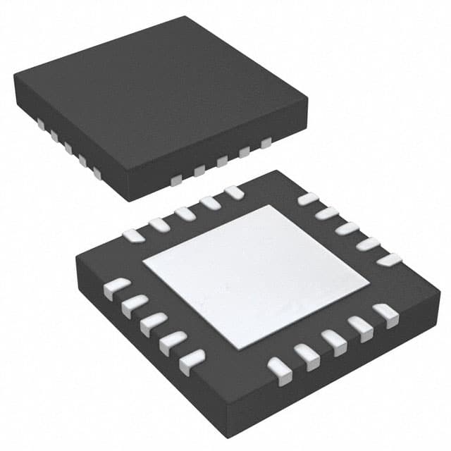
20-UFQFN Exposed Pad
Datasheet:
AetrixSX1501I087TRT.pdf
Description:
IC XPNDR 400KHZ I2C 20QFN
Quantity:
Payment:
Payment
Shipping:
Shipping

Inventory:2,476

Please send an inquiry. Send us your inquiry, and we will respond immediately.

Part Number
Quantity*
Price
Name*
Company
Email*
Comments

Product details

Overview

SX1501I087TRT from Semtech is a 4-channel ultra-low-voltage GPIO expander with I²C interface, NINT interrupt output, and NRESET input. It operates with core voltage as low as 1.2V, independent I/O banks (VCC1) from 1.2V to 5.5V, supports up to 24mA sink per high-sink I/O pin, and delivers typ. 1µA supply current in idle mode. It serves as level shifter and programmable logic block (PLD) in space-constrained battery-powered handhelds.

For engineers reviewing the SX1501I087TRT datasheet, pinout, applications, or equivalent options, key selection criteria include its QFN-UT-20 package footprint, 400kHz I²C slave compatibility, maskable edge-triggered interrupt (NINT), dual-supply independence (VDDM/VCC1), and programmable pull-up/pull-down per I/O - all critical for low-power portable system I/O expansion.

Technical Context

The SX1501I087TRT implements a register-mapped I²C slave interface (7-bit address 0x20/0x21) with 12 user-accessible 8-bit configuration registers, supporting read/write operations without auto-increment (unlike SX1503). Its internal architecture includes independent power domains: VDDM (1.2–5.5V) for core logic and NRESET/NINT, and VCC1 (1.2–5.5V) for all four I/O pins (I/O[0]–I/O[3]), enabling true level-shifting between disparate voltage rails.

Each I/O is fully programmable for direction, pull-up/down strength (~60kΩ at 5V), push-pull or open-drain output, and Schmitt-trigger input hysteresis (0.1×VCC1). The device integrates a PLD block for combinational logic synthesis across its 4 pins and generates maskable interrupts on rising/falling edges via dedicated NINT pin - all configurable without external components.

Key Specifications

Parameter Value and Actual Design Meaning
I/O Channels 4 bidirectional, independently configurable GPIOs (I/O[0]–I/O[3])
Supply Voltage Range VDDM = 1.2–5.5V (core); VCC1 = 1.2–5.5V (I/O bank) - enables mixed-voltage system interfacing
I²C Interface 400kHz Fast-mode slave; 7-bit address (0x20 or 0x21 based on ADDR pin); no 10-bit addressing support
Output Sink Current Up to 24mA per high-sink I/O (I/O[2], I/O[3]); 6–12mA for other I/Os - drives LEDs or small loads directly
Quiescent Current Typ. 1µA at VDDM = VCC1 = 3.3V, I²C inactive - extends battery life in always-on monitoring
Interrupt Output Open-drain active-low NINT with per-pin edge masking and <1µs response latency - enables rapid host wake-up
Operating Temperature –40°C to +85°C - qualified for industrial and consumer portable environments

Pinout & Package

Package: QFN-UT-20 (3×3 mm, 0.4 mm pitch), thermally enhanced with exposed GND pad. RoHS-compliant, moisture sensitivity level (MSL) 3.

Pin/Terminal Circuit Role Design Meaning
NRESET Active-low reset input/output Open-drain output during POR; accepts external active-low reset pulse (min. 300ns); requires external pull-up to VDDM
SDA I²C serial data line Open-drain bidirectional I/O compliant with Philips I²C spec v2.1; requires external pull-up
NC1, NC2, NC3, NC4, NC5, NC6, NC7 No-connect terminals NC1/NC2/NC3/NC4/NC5/NC6 must be left floating; NC7 must be connected to VCC1 per datasheet
SCL I²C serial clock input CMOS input with hysteresis; supports 400kHz max clock frequency
I/O[0]–I/O[3] Programmable GPIOs All four pins support input, output, pull-up/down, Schmitt trigger, and interrupt enable - I/O[2]/I/O[3] support high-sink mode
VCC1 I/O supply rail Independent 1.2–5.5V supply for all I/O pins - decouples I/O logic from core voltage
VDDM Main supply rail 1.2–5.5V supply for core logic, NRESET, NINT, and I²C interface - powers internal registers and state machine
ADDR I²C address select Connect to GND → 0x20; connect to VDDM → 0x21 - enables two devices on same bus
NINT Interrupt output Open-drain active-low output indicating masked edge transitions on any enabled I/O - requires external pull-up
GND (Pins 8, 18, PAD) Ground reference Three dedicated ground connections plus thermal pad - ensures low-impedance return path and thermal dissipation

Key Features

Feature Design Value
Independent dual-supply operation VDDM and VCC1 each support 1.2–5.5V - enables seamless interfacing between 1.8V microcontrollers and 3.3V/5V peripherals
Programmable logic (PLD) Configurable combinational logic across all 4 I/Os - replaces discrete gates in keypad scanning, LED sequencing, or status encoding
Maskable edge-triggered interrupt NINT asserts only on selected rising/falling edges of enabled I/Os - reduces host polling and false wake-ups
High-sink I/O capability I/O[2] and I/O[3] deliver up to 24mA sink at 5.5V - directly drives RGB LEDs or small relays without external drivers
Ultra-low static current 1µA typical IDD at 3.3V - preserves battery charge in sleep-mode applications like remote controls or wearables

Applications

Cell Phone Keypad Interface Portable Media Player LED Control

Use Scenario: Scanning a 4×4 mechanical keypad matrix in a slim smartphone form factor with tight power budget.

IC Role / Device Role / Timing Role: SX1501I087TRT acts as I²C-connected keypad scanner, using its PLD to encode row/column states and NINT to signal keypress events to the AP.

Use Value: Eliminates need for dedicated keypad controller IC and reduces firmware overhead - leverages built-in Schmitt triggers and programmable debounce.

Use Scenario: Driving backlight and status LEDs in an MP3 player with varying supply voltages (1.8V SoC, 3.3V display).

IC Role / Device Role / Timing Role: SX1501I087TRT serves as level-shifting LED driver, sourcing/sinking current from VCC1 while controlled via I²C from low-voltage host.

Use Value: Enables direct LED control without external level shifters or MOSFETs - high-sink I/Os drive 20mA LEDs at 3.3V with <0.3V VOL.

Industrial Sensor Hub I/O Expansion GPS Tracker Status Monitoring

Use Scenario: Adding digital inputs for limit switches and outputs for relay control in a compact GPS tracking module operating at –40°C to +85°C.

IC Role / Device Role / Timing Role: SX1501I087TRT provides isolated, ESD-hardened (1500V HBM) I/O expansion with NRESET synchronization to main MCU.

Use Value: Guarantees reliable operation across full industrial temperature range - VCC1/VDDM independence prevents latch-up during rail sequencing.

Use Scenario: Monitoring battery voltage, SIM presence, and antenna connection status in a battery-backed GPS tracker with aggressive sleep cycling.

IC Role / Device Role / Timing Role: SX1501I087TRT functions as always-on status monitor, using NINT to wake host MCU only on critical state changes.

Use Value: Reduces average system current by >90% versus polling - 1µA quiescent draw extends months-long battery life.

Equivalent & Alternatives

The following parts are listed as comparable options for similar GPIO expander applications.

Alternative Part Technical Difference Application Difference Selection Advice
TCA6408A 8-channel, fixed 1.65–5.5V VCC, no PLD, no high-sink I/Os, 100kHz/400kHz I²C Lacks programmable logic and high-current drive - suitable only for basic I/O extension without local processing Choose TCA6408A when channel count >4 is needed and PLD/high-sink features are unnecessary
PCA9554A 8-channel, 2.3–5.5V VCC, no PLD, no NINT masking, 100kHz I²C only, 10mA max sink Lower integration, no edge-selectable interrupt, narrower voltage range - limits use in ultra-low-VDD designs Choose PCA9554A for legacy 100kHz systems where cost is prioritized over flexibility and low-voltage operation

Compared with TCA6408A and PCA9554A, the SX1501I087TRT uniquely combines 4-channel optimization, sub-1.8V operation, integrated PLD logic, and 24mA high-sink capability - making it the only choice for space- and power-constrained designs requiring autonomous I/O behavior.

Availability

SX1501I087TRT is available at Aetrix Electronics and suitable for portable electronics, industrial sensor nodes, and GPS tracking modules requiring stable component supply, long-term lifecycle support, and RoHS-compliant packaging.

Supply support for SX1501I087TRT includes scheduled delivery planning, volume procurement assistance, BOM continuity management, traceable sourcing, and lifecycle availability coordination for OEM customers, industrial embedded developers, connected-device designers, and electronics production programs.

Manufacturer

Semtech Corporation is a U.S.-based semiconductor company specializing in analog and mixed-signal ICs for precision sensing, power management, and high-performance communications.

The SX1501I087TRT belongs to Semtech's low-voltage GPIO expander family, designed specifically for battery-powered portable equipment needing intelligent, space-efficient I/O expansion with minimal external components.

FAQ

What is the function of the NC7 pin on the SX1501I087TRT?

The NC7 pin on the SX1501I087TRT is not a no-connect - it must be externally connected to VCC1 per the official datasheet (Rev 7, p.4). This connection stabilizes internal biasing for the I/O bank and ensures reliable operation across the full 1.2–5.5V VCC1 range. Leaving NC7 unconnected may cause undefined I/O behavior or increased leakage current in the SX1501I087TRT.

Does the SX1501I087TRT support auto-increment during I²C register reads?

No, the SX1501I087TRT does not support I²C register auto-increment during reads or writes - unlike the SX1503. Each register access requires explicit 8-bit address transmission before data transfer. This is confirmed in Section 4.5.1 and 4.5.2 of the datasheet, which specify "no auto increment/decrement capability" for SX1501 and SX1502 variants. Firmware must manually sequence register addresses when reading multiple SX1501I087TRT registers.

Can the SX1501I087TRT operate with VDDM = 1.2V and VCC1 = 5.0V simultaneously?

Yes, the SX1501I087TRT explicitly supports independent supply rails: VDDM can be as low as 1.2V while VCC1 is set to 5.0V. This dual-rail capability is a core feature validated in Electrical Specifications Table 5 (p.7), enabling the SX1501I087TRT to act as a level shifter between ultra-low-voltage controllers (e.g., 1.2V ARM cores) and 5V peripherals - with full functionality including 24mA sink on I/O[2]/I/O[3].

What is the maximum sink current capability of I/O[0] and I/O[1] on the SX1501I087TRT?

I/O[0] and I/O[1] on the SX1501I087TRT support up to 12mA sink current when VCC1 ≥ 2V and Boost Mode is enabled (RegAdvanced bit 1 = 1), per Table 6 (p.9). In default (Boost Mode off) operation, their sink capability is 6mA. This is distinct from I/O[2] and I/O[3], which support 24mA under the same conditions - a hardware-differentiated feature documented in Pin Description Table 1 (p.4).

How is the I²C address configured for the SX1501I087TRT?

The I²C address of the SX1501I087TRT is set by the ADDR pin: connecting ADDR to GND selects 0x20 (binary 0100000), while connecting ADDR to VDDM selects 0x21 (binary 0100001). This dual-address capability allows two SX1501I087TRT devices to share the same I²C bus. The address is hardwired at power-on and cannot be changed dynamically in software.

SX1501I087TRT Specifications

Product attributes
Attribute value
Manufacturer:
Semtech Corporation
Series:
-
Package/Case:
20-UFQFN Exposed Pad
Packaging:
Tape & Reel (TR)
Product Status:
Obsolete
Programmable:
Not Verified
Number of I/O:
4
Interface:
I2C
Interrupt Output:
Yes
Features:
POR
Output Type:
Push-Pull
Current - Output Source/Sink:
8mA, 24mA
Clock Frequency:
400 kHz
Voltage - Supply:
1.2V ~ 5.5V
Operating Temperature:
-40°C ~ 85°C
Grade:
-
Qualification:
-
Mounting Type:
Surface Mount
Supplier Device Package:
20-QFN-UT (3x3)

SX1501I087TRT FAQ

1.How can I place an order for SX1501I087TRT through Aetrix?

Please submit a Request for Quotation (RFQ) for SX1501I087TRT on Aetrix. Our sales agent will provide a competitive quotation and guide you through the order confirmation once you accept the terms.

2.Are the price and stock information for SX1501I087TRT reliable?

The price and inventory of SX1501I087TRT are updated periodically and may fluctuate due to market conditions. Stock and pricing data are typically refreshed every 24 hours. Quotation validity for SX1501I087TRT is usually 5 days.

3.What payment methods are accepted for SX1501I087TRT?

We accept Wire Transfer, PayPal, Credit Card, Western Union, MoneyGram, and Escrow for SX1501I087TRT transactions.

Note: Certain payment methods may incur a processing fee.

4.How is shipping managed for SX1501I087TRT?

SX1501I087TRT orders can be shipped via leading logistics carriers, including DHL, UPS, FedEx, TNT, or Registered Mail.

Once your SX1501I087TRT order is processed, you will receive an email with the shipment details and tracking number.

Note: Tracking information may take up to 24 hours to appear. Express delivery typically takes 3–5 business days.

5.How can I obtain technical support or documentation for SX1501I087TRT?

For technical support, including SX1501I087TRT datasheets, pinout diagrams, or application guidance, please contact our engineering support team. They can provide detailed documentation and assistance for your SX1501I087TRT requirements.

6.How does Aetrix verify that SX1501I087TRT is sourced from the original manufacturer or authorized distributors?

All SX1501I087TRT products on Aetrix are procured from qualified distributors and authorized channels. Our dedicated quality assurance team conducts strict verification, including traceability checks and, if necessary, third-party testing. This ensures that SX1501I087TRT meets industry standards.

7.What is the process for return or replacement of SX1501I087TRT?

All SX1501I087TRT units undergo pre-shipment inspection (PSI). If there is an issue with SX1501I087TRT, returns or replacements are accepted under the following conditions:

1.Quantity discrepancies, incorrect items, or visible external defects (such as breakage or corrosion), acknowledged by Aetrix.

2.The issue is reported within 90 days of delivery.

3.The SX1501I087TRT part is unused and in its original packaging.

Return procedure for SX1501I087TRT:

1.Submit a request within 90 days.

2.Obtain a Return Material Authorization (RMA) from Aetrix.

SX1501I087TRT Tags
  • SX1501I087TRT
  • SX1501I087TRT PDF
  • SX1501I087TRT Datasheet
  • SX1501I087TRT Specifications
  • SX1501I087TRT Images
  • Semtech Corporation
  • Semtech Corporation SX1501I087TRT
  • Buy SX1501I087TRT
  • SX1501I087TRT Price
  • SX1501I087TRT Distributor
  • SX1501I087TRT Supplier
  • SX1501I087TRT Wholesale
Related Products
TCA6408ARSVR
TCA6408ARSVR

Texas Instruments

TCA9535RTWR
TCA9535RTWR

Texas Instruments

FXL6408UMX
FXL6408UMX

onsemi

PCF8574ADWR
PCF8574ADWR

Texas Instruments

PCF8574APWR
PCF8574APWR

Texas Instruments

TCA9555PWR
TCA9555PWR

Texas Instruments

TCA9554PWR
TCA9554PWR

Texas Instruments

TCA9554APWR
TCA9554APWR

Texas Instruments

TCA9539PWR
TCA9539PWR

Texas Instruments

TCA9534PWR
TCA9534PWR

Texas Instruments

TCA9555RTWR
TCA9555RTWR

Texas Instruments

TCA9535PWR
TCA9535PWR

Texas Instruments

Tech Hub

Search

Search

PRODUCT

PRODUCT

PHONE

PHONE

USER

USER