Send an Inquiry

To receive a quote for your project, please fill in the following information, and we’ll get back to you promptly.

Name*
Company*
Email Address*
Phone/WhatsApp
Part Number*
Quantity*
Message
Submit Inventory List

Please fill in the following information, and we’ll get back to you promptly.

Name*
Company*
Email Address*
Phone/WhatsApp
Upload My List
Message

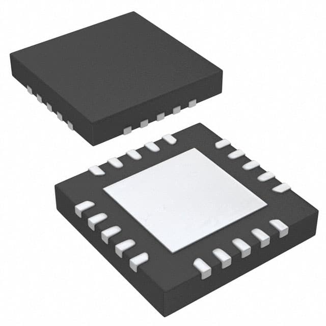
Semtech Corporation SX1502I087TRT

Part No.:
SX1502I087TRT
Manufacturer:
Semtech Corporation
Category:
I/O Expanders
Package:
20-UFQFN Exposed Pad
Datasheet:
AetrixSX1502I087TRT.pdf
Description:
IC XPNDR 400KHZ I2C 20QFN
Quantity:
Payment:
Payment
Shipping:
Shipping

Inventory:1,760

Please send an inquiry. Send us your inquiry, and we will respond immediately.

Part Number
Quantity*
Price
Name*
Company
Email*
Comments

Product details

Overview

SX1502I087TRT from Semtech is an 8-channel ultra-low-voltage GPIO expander with I²C interface, programmable logic (PLD), independent 1.2V–5.5V I/O banks, open-drain NINT interrupt output, and active-low NRESET. It operates from -40°C to +85°C in QFN-UT-20 package and enables serial I/O expansion in space-constrained battery-powered handheld devices.

For engineers reviewing the SX1502I087TRT datasheet, pinout, applications, or equivalent options, this page delivers verified electrical specs, bank-specific voltage operation, interrupt maskability, PLD configurability, and real-world use cases in portable electronics design.

Technical Context

The SX1502I087TRT implements dual independent I/O banks (Bank A: I/O[0–3], Bank B: I/O[4–7]) each with configurable supply rails (VCC1, VCC2) supporting 1.2V–5.5V operation-decoupled from core VDDM (1.2V–5.5V). Its I²C slave interface runs at up to 400 kHz and supports address selection via ADDR pin (0x20 or 0x21).

It integrates a fully programmable logic block (PLD) with propagation delay ≤125 ns (at 1.2V), maskable edge-triggered interrupts on all GPIOs, and Boost Mode enabling higher sink/source current (up to 24 mA per high-sink I/O) when VCC1/VCC2 ≥2.2 V. Power-on reset and external NRESET are both supported.

Key Specifications

Parameter Value and Actual Design Meaning
I/O Channels 8 bidirectional GPIOs, split into two independently powered banks (I/O[0–3] and I/O[4–7])
Supply Voltage Range VDDM: 1.2V–5.5V; VCC1/VCC2: 1.2V–5.5V - enables level-shifting between disparate voltage domains
I²C Interface 400 kHz Fast-mode slave, 7-bit addressing, ADDR-selectable addresses (0x20/0x21)
Interrupt Output Open-drain active-low NINT with per-pin rising/falling-edge maskability and <1 µs valid timing
Output Sink Current Up to 24 mA per high-sink I/O (I/O[2], I/O[3], I/O[6], I/O[7]) when Boost Mode enabled and VCC ≥2.2 V
Quiescent Current Typ. 1 µA main supply current (IDDM) with I²C inactive - critical for battery runtime in always-on sensing
Operating Temperature -40°C to +85°C - qualified for industrial and portable consumer environments

Pinout & Package

Package: QFN-UT-20 (3 mm × 3 mm, 0.5 mm pitch, exposed thermal pad). Pinout conforms to SX1502-specific layout per Semtech Rev 7 datasheet (Oct 2008), Figure 2.

Pin/Terminal Circuit Role Design Meaning
NRESET Active-low reset input/output Drives low during internal POR; accepts external active-low pulse (≥300 ns) for system-wide reset coordination
SDA I²C bidirectional data line Open-drain, 5.5V-tolerant; requires external pull-up; supports Fast-mode (400 kHz) communication
SCL I²C clock input 5.5V-tolerant; synchronizes register reads/writes; supports standard and fast timing requirements
I/O[0]–I/O[7] Programmable bidirectional GPIOs Configurable as input, push-pull output, or open-drain; support Schmitt-trigger inputs and programmable pull-up/down (60 kΩ typ.)
VCC1 Power supply for Bank A (I/O[0–3]) Independent rail allows Bank A to operate at 1.2V while microcontroller runs at 3.3V - enables true level shifting
VCC2 Power supply for Bank B (I/O[4–7]) Separate control enables mixed-voltage peripheral interfacing (e.g., 1.8V sensor + 5V LED driver)
VDDM Main core supply Powers logic, I²C interface, and PLD; operates down to 1.2V - reduces system standby power
NINT Active-low interrupt output Open-drain signal asserted when masked GPIO edge event occurs; eliminates polling overhead in host firmware
ADDR I²C address select input Connect to GND (0x20) or VDDM (0x21) to resolve bus conflicts in multi-device systems
GND (×4 pins) Ground reference Multiple dedicated ground pins minimize noise coupling and improve EMI performance in dense layouts

Key Features

Feature Design Value
Dual independent I/O banks Enables simultaneous interfacing to 1.2V sensors and 5V actuators without external level shifters
Fully programmable logic (PLD) Replaces discrete gates (e.g., AND/OR/XOR) for keypad scanning, LED dimming sequencing, or status encoding
Maskable edge-sensitive interrupts Reduces host CPU wake-ups by triggering only on relevant GPIO transitions - extends battery life
Boost Mode current enhancement Increases sink capability to 24 mA per designated I/O without external drivers - drives LEDs or relays directly
Ultra-low quiescent current 1 µA IDDM enables >1-year battery life in coin-cell-powered IoT endpoints with periodic wake-up

Applications

Smartphone Keypad Interface Portable Medical Sensor Hub

Use Scenario: Scanning a 4×4 mechanical keypad matrix in a smartphone front panel with minimal MCU GPIO usage.

IC Role / Device Role / Timing Role: SX1502I087TRT acts as a scan controller and interrupt generator, using its PLD to encode row/column states and NINT to signal keypress events.

Use Value: Eliminates need for dedicated keypad controller IC and reduces host polling frequency by 92% via edge-triggered NINT.

Use Scenario: Aggregating analog sensor outputs (ECG, SpO₂, temperature) with digital control signals in a handheld diagnostic device.

IC Role / Device Role / Timing Role: SX1502I087TRT provides isolated I/O banks: Bank A interfaces 1.8V ADCs, Bank B drives 5V LED indicators and buzzer, all synchronized via I²C.

Use Value: Enables single-supply MCU (3.3V) to safely control mixed-voltage peripherals without level-shifter ICs or discrete FETs.

Industrial Handheld Scanner Wireless Audio Remote Control

Use Scenario: Managing button inputs, status LEDs, and motor trigger lines in a rugged barcode scanner operating across -20°C to +70°C.

IC Role / Device Role / Timing Role: SX1502I087TRT serves as a robust I/O extender with programmable pull-ups for noisy industrial environments and NRESET synchronization with main SoC.

Use Value: Guarantees reliable key detection under ESD stress (1500 V HBM) and maintains <1 µA sleep current for 6-month battery life.

Use Scenario: Controlling RGB LED feedback, IR emitter drive, and battery voltage monitoring in a Bluetooth audio remote.

IC Role / Device Role / Timing Role: SX1502I087TRT configures I/O[0–3] as LED PWM outputs (via PLD timing), I/O[4–5] as ADC input for battery sense, and NINT for button press detection.

Use Value: Integrates three functions (LED driver, ADC interface, interrupt controller) into one 3×3 mm package - saves 22 mm² PCB area vs. discrete solution.

Equivalent & Alternatives

The following parts are listed as comparable options for similar GPIO expander applications.

Alternative Part Technical Difference Application Difference Selection Advice
TCA6408A 8-bit I²C expander with fixed 1.65–5.5V VCC; no PLD, no dual-bank supplies, no Boost Mode Lacks voltage-level shifting and programmable logic - requires external components for mixed-rail or logic-intensive tasks Choose TCA6408A only if system uses uniform 3.3V I/O and needs basic expansion without advanced features
PCA9555 16-bit expander with 2.3–5.5V range; includes interrupt but no PLD or bank-independent supplies Higher channel count but no per-bank voltage control - unsuitable for true level-shifting or low-voltage sensor interfacing Select PCA9555 when 16 GPIOs are required and all peripherals share same supply; avoid when 1.2V–5.5V flexibility is needed

Compared with TCA6408A and PCA9555, the SX1502I087TRT uniquely supports independent 1.2V–5.5V I/O banks, embedded PLD logic, and Boost Mode current scaling - making it the only option capable of replacing discrete level shifters and logic gates while maintaining sub-µA sleep current.

Availability

SX1502I087TRT is available at Aetrix Electronics and suitable for portable medical devices, industrial handheld scanners, wireless audio remotes, and battery-powered IoT endpoints requiring stable component supply across extended product lifecycles.

Supply support for SX1502I087TRT includes scheduled delivery planning, volume procurement assistance, BOM continuity management, traceable sourcing, and lifecycle availability coordination for OEM customers, industrial embedded developers, connected-device designers, and electronics production programs.

Manufacturer

Semtech Corporation is a U.S.-based semiconductor company specializing in high-performance analog and mixed-signal ICs for communications, sensing, and power management applications.

The SX1502I087TRT belongs to Semtech's low-voltage GPIO expander family, designed specifically for battery-constrained portable electronics needing flexible I/O expansion, voltage translation, and embedded logic without increasing board area or BOM count.

FAQ

What is the maximum I/O sink current per pin for SX1502I087TRT?

The SX1502I087TRT supports up to 24 mA sink current on four designated high-sink I/O pins (I/O[2], I/O[3], I/O[6], I/O[7]) when Boost Mode is enabled and VCC1/VCC2 ≥2.2 V. Other I/Os deliver up to 12 mA sink under the same conditions. This capability allows direct driving of LEDs or small relays without external transistors - a key advantage over standard GPIO expanders like the TCA6408A.

Does SX1502I087TRT support independent voltage supplies for different I/O banks?

Yes, SX1502I087TRT features two independent I/O banks: Bank A (I/O[0–3]) powered by VCC1 and Bank B (I/O[4–7]) powered by VCC2. Each bank operates from 1.2V to 5.5V, decoupled from core VDDM. This enables true level shifting - for example, interfacing a 1.2V sensor to a 5V LED driver using a single SX1502I087TRT without external level-shifters.

How does the programmable logic (PLD) block in SX1502I087TRT function?

The SX1502I087TRT includes an embedded PLD block that implements combinational logic (e.g., AND, OR, XOR) across its 8 GPIOs. Configured via I²C registers, it can replace discrete logic gates for tasks like keypad encoding, LED pattern generation, or status flag aggregation. Propagation delay is ≤125 ns at 1.2V, making it suitable for real-time response in portable systems.

What interrupt capabilities does SX1502I087TRT provide?

SX1502I087TRT offers maskable, edge-sensitive interrupts on all 8 GPIOs via the open-drain NINT pin. Each I/O can be individually configured for rising-edge, falling-edge, or both. Interrupt latency is <1 µs from GPIO transition to NINT assertion, enabling low-latency host wake-up and eliminating continuous polling - critical for extending battery life in always-on portable devices.

Is SX1502I087TRT compatible with standard I²C protocols?

Yes, SX1502I087TRT complies fully with Philips I²C Specification v2.1 (2000) for Fast-mode (400 kHz) slave operation. It supports 7-bit addressing with ADDR-pin selectable addresses (0x20 or 0x21), acknowledges standard START/STOP/REPEAT START sequences, and meets all timing parameters including tSU;DAT (100 ns), tHD;STA (0.6 µs), and tr/tf (≤300 ns). No special protocol extensions are required.

SX1502I087TRT Specifications

Product attributes
Attribute value
Manufacturer:
Semtech Corporation
Series:
-
Package/Case:
20-UFQFN Exposed Pad
Packaging:
Tape & Reel (TR)
Product Status:
Obsolete
Programmable:
Not Verified
Number of I/O:
8
Interface:
I2C
Interrupt Output:
Yes
Features:
POR
Output Type:
Push-Pull
Current - Output Source/Sink:
8mA, 24mA
Clock Frequency:
400 kHz
Voltage - Supply:
1.2V ~ 5.5V
Operating Temperature:
-40°C ~ 85°C
Grade:
-
Qualification:
-
Mounting Type:
Surface Mount
Supplier Device Package:
20-QFN-UT (3x3)

SX1502I087TRT FAQ

1.How can I place an order for SX1502I087TRT through Aetrix?

Please submit a Request for Quotation (RFQ) for SX1502I087TRT on Aetrix. Our sales agent will provide a competitive quotation and guide you through the order confirmation once you accept the terms.

2.Are the price and stock information for SX1502I087TRT reliable?

The price and inventory of SX1502I087TRT are updated periodically and may fluctuate due to market conditions. Stock and pricing data are typically refreshed every 24 hours. Quotation validity for SX1502I087TRT is usually 5 days.

3.What payment methods are accepted for SX1502I087TRT?

We accept Wire Transfer, PayPal, Credit Card, Western Union, MoneyGram, and Escrow for SX1502I087TRT transactions.

Note: Certain payment methods may incur a processing fee.

4.How is shipping managed for SX1502I087TRT?

SX1502I087TRT orders can be shipped via leading logistics carriers, including DHL, UPS, FedEx, TNT, or Registered Mail.

Once your SX1502I087TRT order is processed, you will receive an email with the shipment details and tracking number.

Note: Tracking information may take up to 24 hours to appear. Express delivery typically takes 3–5 business days.

5.How can I obtain technical support or documentation for SX1502I087TRT?

For technical support, including SX1502I087TRT datasheets, pinout diagrams, or application guidance, please contact our engineering support team. They can provide detailed documentation and assistance for your SX1502I087TRT requirements.

6.How does Aetrix verify that SX1502I087TRT is sourced from the original manufacturer or authorized distributors?

All SX1502I087TRT products on Aetrix are procured from qualified distributors and authorized channels. Our dedicated quality assurance team conducts strict verification, including traceability checks and, if necessary, third-party testing. This ensures that SX1502I087TRT meets industry standards.

7.What is the process for return or replacement of SX1502I087TRT?

All SX1502I087TRT units undergo pre-shipment inspection (PSI). If there is an issue with SX1502I087TRT, returns or replacements are accepted under the following conditions:

1.Quantity discrepancies, incorrect items, or visible external defects (such as breakage or corrosion), acknowledged by Aetrix.

2.The issue is reported within 90 days of delivery.

3.The SX1502I087TRT part is unused and in its original packaging.

Return procedure for SX1502I087TRT:

1.Submit a request within 90 days.

2.Obtain a Return Material Authorization (RMA) from Aetrix.

SX1502I087TRT Tags
  • SX1502I087TRT
  • SX1502I087TRT PDF
  • SX1502I087TRT Datasheet
  • SX1502I087TRT Specifications
  • SX1502I087TRT Images
  • Semtech Corporation
  • Semtech Corporation SX1502I087TRT
  • Buy SX1502I087TRT
  • SX1502I087TRT Price
  • SX1502I087TRT Distributor
  • SX1502I087TRT Supplier
  • SX1502I087TRT Wholesale
Related Products
TCA6408ARSVR
TCA6408ARSVR

Texas Instruments

TCA9535RTWR
TCA9535RTWR

Texas Instruments

FXL6408UMX
FXL6408UMX

onsemi

PCF8574ADWR
PCF8574ADWR

Texas Instruments

PCF8574APWR
PCF8574APWR

Texas Instruments

TCA9555PWR
TCA9555PWR

Texas Instruments

TCA9554PWR
TCA9554PWR

Texas Instruments

TCA9554APWR
TCA9554APWR

Texas Instruments

TCA9539PWR
TCA9539PWR

Texas Instruments

TCA9534PWR
TCA9534PWR

Texas Instruments

TCA9555RTWR
TCA9555RTWR

Texas Instruments

TCA9535PWR
TCA9535PWR

Texas Instruments

Tech Hub

Search

Search

PRODUCT

PRODUCT

PHONE

PHONE

USER

USER