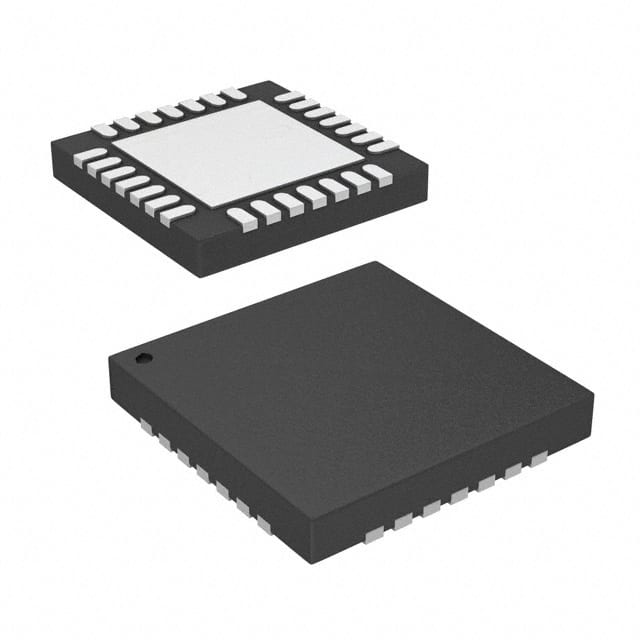
Semtech Corporation SX1506I091TRT
- Part No.:
- SX1506I091TRT
- Manufacturer:
- Semtech Corporation
- Category:
- I/O Expanders
- Package:
- 28-UFQFN Exposed Pad
- Datasheet:
-
SX1506I091TRT.pdf
- Description:
- IC XPNDR 400KHZ I2C 28QFN
- Quantity:
- Payment:

- Shipping:

Inventory:2,288
Please send an inquiry. Send us your inquiry, and we will respond immediately.
Product details
Overview
SX1506I091TRT from Semtech is a 16-channel programmable GPIO expander with I²C interface, NINT interrupt output, and NRESET input. It operates with core voltage (VDDM) from 2.5V to 5.5V and dual independent I/O banks (VCC1/VCC2) at 2.5V–5.5V, supports up to 24mA sink per high-sink I/O pin, and delivers ultra-low standby current (1µA typ). It enables I/O expansion in space-constrained, battery-powered handheld devices such as GPS units and portable multimedia players.
For engineers reviewing the SX1506I091TRT datasheet, pinout, applications, or equivalent options, key selection considerations include its QFN-UT-28 package, 400kHz I²C slave interface, maskable edge-triggered interrupts, fully programmable PLD logic for combinational functions, and dual-voltage I/O bank isolation for level-shifting between subsystems.
Technical Context
The SX1506I091TRT implements a 16-bit parallel I/O expansion architecture with two independent 8-bit I/O banks (Bank A: I/O[0–7], Bank B: I/O[8–15]), each configurable via dedicated VCC1 and VCC2 supplies. Its internal register map includes 31 user-accessible 8-bit registers supporting direction, pull-up/pull-down, interrupt masking/sensing, and PLD configuration.
It integrates a fully programmable PLD block capable of implementing up to four 3-to-1 or two 3-to-2 combinational logic functions across selected I/O pins, while retaining full GPIO functionality on non-PLD pins. The device features auto-incrementing register addressing during I²C read/write sequences - a capability exclusive to the SX1506 within the family - improving firmware efficiency in multi-register access.
Key Specifications
| Parameter | Value and Actual Design Meaning |
|---|---|
| I/O Channels | 16 bidirectional, individually configurable GPIOs grouped into two 8-bit banks |
| I²C Interface | 400kHz Fast-mode slave-only interface with fixed 7-bit address 0x20; supports auto-increment register addressing |
| VDDM Supply Range | 2.5V to 5.5V - powers core logic and reset/interrupt circuitry |
| VCC1 / VCC2 Range | 2.5V to 5.5V - independently configurable for Bank A and Bank B I/O voltage levels |
| Output Sink Current | Up to 24mA per designated high-sink I/O pin (I/O[2,3,6,7,14,15]); no total sink limit |
| Standby Current | 1µA typical at VDDM = 3.3V, I²C inactive - enables long battery life in portable systems |
| Interrupt Output | Open-drain active-low NINT with bit-maskable rising/falling-edge sensitivity per GPIO |
| PLD Capability | Fully programmable truth-table logic supporting up to four 3-to-1 or two 3-to-2 combinational functions |
Pinout & Package
The SX1506I091TRT is housed in a 4×4 mm, 0.5 mm pitch, ultra-thin QFN-UT-28 package with exposed thermal pad (GND). All pins are surface-mount; pin 1 is GND (top-left corner, marked by dot).
| Pin/Terminal | Circuit Role | Design Meaning |
|---|---|---|
| 1, 7, 15, 21, GND Pad | Ground reference | Five separate GND connections ensure low-impedance return paths for core, I/O banks, and thermal dissipation |
| 2–6, 8–9, 13–14, 16–20, 22–23, 27–28 | Programmable I/O[0–15] | 16 bidirectional pins; I/O[2,3,6,7,14,15] support 24mA sink; all configurable as input/output/push-pull/open-drain |
| 4, 18 | VCC1 / VCC2 | Independent power supplies for Bank A (I/O[0–7]) and Bank B (I/O[8–15]); enable level-shifting between subsystems |
| 12 | VDDM | Main supply for internal logic, I²C interface, reset, and interrupt circuitry |
| 10 | NINT | Open-drain active-low interrupt output; signals state change on any masked GPIO edge |
| 24 | NRESET | Active-low reset input/output; driven low internally during POR; accepts external reset pulses ≥300ns |
| 25–26 | SDA / SCL | I²C serial data and clock lines; compliant with Philips I²C v2.1 Fast-mode (400kHz) |
| 11 | NC | No-connect pin - must be left floating per datasheet |
Key Features
| Feature | Design Value |
|---|---|
| Dual independent I/O voltage banks | VCC1 and VCC2 each support 2.5V–5.5V operation, enabling seamless level translation between host MCU and peripheral ICs |
| Maskable edge-triggered interrupts | NINT asserts on rising/falling edges of any combination of 16 GPIOs; RegInterruptSource identifies triggering pins |
| On-chip programmable logic (PLD) | Configurable truth-table logic allows implementation of custom AND/OR/decode functions without external gates |
| Auto-increment I²C addressing | Enables efficient burst reads/writes across multiple registers - unique to SX1506 among family members |
| Ultra-low-power standby mode | 1µA typical IDD at 3.3V eliminates need for external power gating in always-on portable applications |
| Robust reset architecture | Integrated POR with VPOR = 0.7–0.9V and brown-out detection (VDROPL/VDROPH) ensures reliable initialization under varying supply conditions |
Applications
| Smartphone Keypad Interface | LED Backlight Control |
|---|---|
Use Scenario: Scanning a 4×4 mechanical keypad matrix in a compact smartphone design where main SoC lacks sufficient GPIOs. IC Role / Device Role / Timing Role: SX1506I091TRT acts as an I²C-controlled keypad scanner, debouncing inputs and generating NINT on keypress/release. Use Value: Reduces host CPU polling overhead, enables wake-from-sleep on key event, and isolates 3.3V SoC from 5V keypad backlight circuitry via VCC1/VCC2 separation. | Use Scenario: Driving 16 individual LED segments in a portable media player's status display with adjustable brightness. IC Role / Device Role / Timing Role: SX1506I091TRT configures I/O[0–15] as push-pull outputs with programmable current limiting; uses PLD logic to synchronize segment enable timing. Use Value: Eliminates need for external LED driver ICs and discrete timing logic; achieves uniform dimming using register-based current control per channel. |
| Industrial Sensor Hub | GPS Module Power Sequencing |
Use Scenario: Aggregating digital status signals (motion, door open, tamper detect) from 12 sensors in a battery-powered asset tracker. IC Role / Device Role / Timing Role: SX1506I091TRT monitors sensor outputs as inputs, masks interrupts for specific events, and reports changes over I²C to host MCU. Use Value: Enables low-duty-cycle monitoring: host sleeps until NINT triggers, reducing system-wide power consumption by >90% versus continuous polling. | Use Scenario: Managing power-up sequencing and fault signaling between baseband processor and GPS RF module in a navigation device. IC Role / Device Role / Timing Role: SX1506I091TRT uses PLD logic to generate precise enable/disable strobes based on processor GPIOs and GPS READY signal. Use Value: Replaces 3 discrete logic ICs and RC timing networks; guarantees sub-microsecond coordination between power rails and communication handshakes. |
Equivalent & Alternatives
The following parts are listed as comparable options for similar GPIO expander applications.
| Alternative Part | Technical Difference | Application Difference | Selection Advice |
|---|---|---|---|
| TCA6424ARGCR | 24-channel I²C expander; no PLD; 25mA sink; requires external pull-ups; no NRESET output | Lacks integrated reset generation and programmable logic; suited for simple I/O extension without timing-critical logic | Select when higher channel count is required and PLD/level-shifting are unnecessary |
| PCA9555DWR | 16-channel I²C expander; no PLD; 10mA sink; fixed 2.3–5.5V VDD; no dual I/O supplies | Cannot perform level translation between subsystems; lower drive strength limits LED/load driving capability | Choose for cost-sensitive designs where dual-voltage operation and high-current I/O are not needed |
Compared with TCA6424ARGCR and PCA9555DWR, the SX1506I091TRT uniquely combines 16-channel expansion with dual independent I/O voltage rails, on-die PLD logic, and integrated NRESET/NINT - enabling single-chip solutions for complex power sequencing, keypad scanning, and mixed-voltage peripheral interfacing without external components.
Availability
SX1506I091TRT is available at Aetrix Electronics and suitable for portable multimedia players, GPS navigation units, and industrial sensor hubs requiring stable component supply, long-term lifecycle support, and RoHS-compliant packaging.
Supply support for SX1506I091TRT includes scheduled delivery planning, volume procurement assistance, BOM continuity management, traceable sourcing, and lifecycle availability coordination for OEM customers, industrial embedded developers, connected-device designers, and electronics production programs.
Manufacturer
Semtech Corporation is a U.S.-based semiconductor company specializing in analog and mixed-signal ICs for precision sensing, wireless infrastructure, and power management.
The SX1506I091TRT belongs to Semtech's Wireless & Sensing product line, designed specifically for low-power, space-constrained portable electronics requiring intelligent I/O expansion with embedded logic and flexible voltage domain interfacing.
FAQ
What is the package type and footprint of the SX1506I091TRT?
The SX1506I091TRT uses a 4×4 mm, 0.5 mm pitch QFN-UT-28 package with an exposed thermal pad (GND). It has 28 terminals including five GND pins (pins 1, 7, 15, 21, and the center pad) for optimal grounding and thermal performance. Land pattern dimensions and soldering profile are specified in Semtech's Packaging Information section (Rev 3, May 2012).
Does the SX1506I091TRT support level shifting between different voltage domains?
Yes, the SX1506I091TRT supports true level shifting via independent VCC1 and VCC2 supplies (2.5V–5.5V each), allowing Bank A (I/O[0–7]) and Bank B (I/O[8–15]) to operate at different voltages than VDDM and each other. This enables direct interfacing between, for example, a 1.8V microcontroller and 5V peripherals without external level translators - a core capability confirmed in the General Description and Electrical Characteristics sections.
How does the programmable logic (PLD) function work in the SX1506I091TRT?
The SX1506I091TRT includes a fully programmable PLD block that implements combinational logic using user-defined truth tables. It supports configurations such as four 3-to-1 or two 3-to-2 logic functions across selected I/O pins. PLD inputs and outputs retain interrupt capability, and non-PLD pins remain fully functional as GPIOs. Configuration is done via RegPLDMode and associated truth table registers, as detailed in Section 4.7.3 of the datasheet.
What are the key differences between SX1506I091TRT and SX1504/SX1505 variants?
The SX1506I091TRT provides 16 GPIOs in QFN-UT-28, whereas SX1504/SX1505 offer 4/8 channels in QFN-UT-20. Only the SX1506 supports I²C register auto-increment, has two full 8-bit I/O banks with dedicated VCC1/VCC2, and implements the most advanced PLD configuration (up to two 3-to-2 functions). Its pinout and register map are distinct - it is not pin-compatible with SX1504 or SX1505.
Can the SX1506I091TRT generate interrupts on both rising and falling edges simultaneously?
Yes, the SX1506I091TRT supports independent rising- and falling-edge sensitivity per GPIO via the RegSenseLow and RegSenseHigh registers. Each I/O can be configured to trigger NINT on either edge, both edges, or neither - all under software control. Interrupt sources are identified by reading RegInterruptSource, and the interrupt is cleared by writing 0xFF to that register or (optionally) by reading RegData when RegAdvanced[7] = 1.
SX1506I091TRT Specifications
- Product attributes
- Attribute value
- Manufacturer:
- Semtech Corporation
- Series:
- -
- Package/Case:
- 28-UFQFN Exposed Pad
- Packaging:
- Tape & Reel (TR)
- Product Status:
- Obsolete
- Programmable:
- Not Verified
- Number of I/O:
- 16
- Interface:
- I2C
- Interrupt Output:
- Yes
- Features:
- POR
- Output Type:
- Push-Pull
- Current - Output Source/Sink:
- 8mA, 24mA
- Clock Frequency:
- 400 kHz
- Voltage - Supply:
- 2.5V ~ 5.5V
- Operating Temperature:
- -40°C ~ 85°C
- Grade:
- -
- Qualification:
- -
- Mounting Type:
- Surface Mount
- Supplier Device Package:
- 28-QFN-UT (4x4)
SX1506I091TRT FAQ
1.How can I place an order for SX1506I091TRT through Aetrix?
Please submit a Request for Quotation (RFQ) for SX1506I091TRT on Aetrix. Our sales agent will provide a competitive quotation and guide you through the order confirmation once you accept the terms.
2.Are the price and stock information for SX1506I091TRT reliable?
The price and inventory of SX1506I091TRT are updated periodically and may fluctuate due to market conditions. Stock and pricing data are typically refreshed every 24 hours. Quotation validity for SX1506I091TRT is usually 5 days.
3.What payment methods are accepted for SX1506I091TRT?
We accept Wire Transfer, PayPal, Credit Card, Western Union, MoneyGram, and Escrow for SX1506I091TRT transactions.
Note: Certain payment methods may incur a processing fee.
4.How is shipping managed for SX1506I091TRT?
SX1506I091TRT orders can be shipped via leading logistics carriers, including DHL, UPS, FedEx, TNT, or Registered Mail.
Once your SX1506I091TRT order is processed, you will receive an email with the shipment details and tracking number.
Note: Tracking information may take up to 24 hours to appear. Express delivery typically takes 3–5 business days.
5.How can I obtain technical support or documentation for SX1506I091TRT?
For technical support, including SX1506I091TRT datasheets, pinout diagrams, or application guidance, please contact our engineering support team. They can provide detailed documentation and assistance for your SX1506I091TRT requirements.
6.How does Aetrix verify that SX1506I091TRT is sourced from the original manufacturer or authorized distributors?
All SX1506I091TRT products on Aetrix are procured from qualified distributors and authorized channels. Our dedicated quality assurance team conducts strict verification, including traceability checks and, if necessary, third-party testing. This ensures that SX1506I091TRT meets industry standards.
7.What is the process for return or replacement of SX1506I091TRT?
All SX1506I091TRT units undergo pre-shipment inspection (PSI). If there is an issue with SX1506I091TRT, returns or replacements are accepted under the following conditions:
1.Quantity discrepancies, incorrect items, or visible external defects (such as breakage or corrosion), acknowledged by Aetrix.
2.The issue is reported within 90 days of delivery.
3.The SX1506I091TRT part is unused and in its original packaging.
Return procedure for SX1506I091TRT:
1.Submit a request within 90 days.
2.Obtain a Return Material Authorization (RMA) from Aetrix.
SX1506I091TRT Tags
-
TCA6408ARSVR
Texas Instruments

-
TCA9535RTWR
Texas Instruments
-
FXL6408UMX
onsemi

-
PCF8574ADWR
Texas Instruments

-
PCF8574APWR
Texas Instruments
-
TCA9555PWR
Texas Instruments

-
TCA9554PWR
Texas Instruments
-
TCA9554APWR
Texas Instruments

-
TCA9539PWR
Texas Instruments
-
TCA9534PWR
Texas Instruments
-
TCA9555RTWR
Texas Instruments

-
TCA9535PWR
Texas Instruments
Tech Hub

Comparator circuit design covering voltage thresholds, input limits, open-collector outputs, LM393 wiring, op-amp differences, hysteresis, timing, window detection and practical fault diagnosis.
Schmitt triggers use separate rising and falling thresholds to stabilize slow or noisy signals. This guide covers hysteresis, 74HC14 and 74HCT14 selection, comparator calculations, RC oscillators and p…
Counterfeit components can hide behind convincing markings and passing basic function tests. This engineering reference covers source traceability, external inspection, X-ray, XRF, electrical testing, …
A practical engineering and sourcing framework covering lifecycle verification, lifetime-buy calculations, replacement qualification, supplier checks and counterfeit-risk controls.
TTL and CMOS logic families differ in thresholds, loading, output drive, power and timing. This engineering guide compares 74HC and 74HCT, calculates noise margins and checks 3.3 V/5 V compatibility.
A practical engineering guide to 3.3V and 5V logic compatibility, input thresholds, resistor dividers, translator ICs, MOSFET level shifting, I2C pull-ups, timing limits and power-sequencing risks.
The 74HC595 uses push-pull logic outputs, while the TPIC6B595 uses 50 V open-drain DMOS sinks for higher-power loads. This guide compares timing, current limits, 3.3 V interfacing, load wiring, thermal…
The 74HC595 converts serial data into eight stable parallel outputs. This guide covers pin functions, shift and storage timing, OE and MR behavior, drive-current limits, cascading, voltage compatibilit…
A technical comparison of level-sensitive latches and edge-triggered flip-flops, covering timing windows, setup and hold limits, master–slave operation, time borrowing, race-through, HDL inference and…
A D latch stores one bit while Enable controls when data can pass. This reference covers gate-level operation, truth tables, transparency, setup and hold timing, LE versus OE, common ICs and practical …