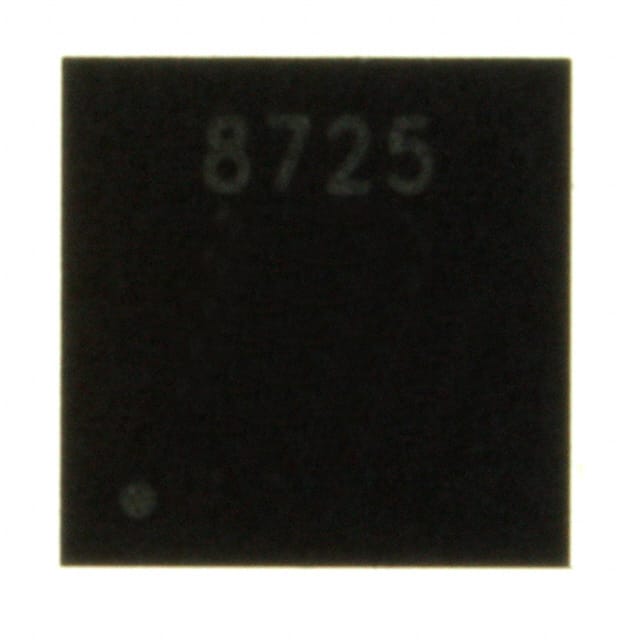
Semtech Corporation SX8725E083TRT
- Part No.:
- SX8725E083TRT
- Manufacturer:
- Semtech Corporation
- Category:
- Sensor and Detector Interfaces
- Package:
- 12-WFDFN Exposed Pad
- Datasheet:
-
SX8725E083TRT.pdf
- Description:
- IC DAS PRESSURE/TEMP SENS 12MLPD
- Quantity:
- Payment:

- Shipping:

Inventory:1,827
Please send an inquiry. Send us your inquiry, and we will respond immediately.
Product details
Overview
SX8725E083TRT from Semtech is a low-power, 16-bit ZoomingADC™ analog-to-digital converter optimized for miniature pressure and temperature sensors. It features one differential analog input (AC2/AC3), two programmable digital I/Os (D0/D1) for sensor biasing or reference handling, and a 2-wire (I²C-compatible) interface operating up to 400 kHz. Its programmable gain (1/12 to 1000), internal 1.22 V bandgap reference, and 250 µA active current at 16-bit/500 S/s enable high-precision sensing in battery-powered industrial transducers.
For engineers reviewing the SX8725E083TRT datasheet, pinout, applications, or equivalent options, this device supports differential sensor interfacing with on-chip PGA offset compensation, selectable power reduction modes, and integrated charge pump for sub-3V operation - critical for compact, low-voltage sensor nodes requiring stable resolution and minimal quiescent current.
Technical Context
The SX8725E083TRT implements a multi-stage programmable gain amplifier (PGA1–PGA3) feeding a sigma-delta ZoomingADC™ core with oversampling ratios from 8 to 1024. Its acquisition chain supports continuous-time or on-request conversion, with resolution dynamically configurable from 6 to 16 bits via OSR and NELCONV register settings.
It integrates an internal RC oscillator (4 MHz), charge pump (VPUMP) for analog switch supply regulation, and GPIO-controlled reference routing (D0 as VREFOUT, D1 as VREFIN). The READY pin provides synchronous end-of-conversion signaling, and all digital I/Os comply with standard 2-wire timing (tSU;DAT ≥ 100 ns, fSCL ≤ 400 kHz).
Key Specifications
| Parameter | Value and Actual Design Meaning |
|---|---|
| Resolution | 6–16 bits, set via OSR (8–1024) and NELCONV (1–8); 16-bit mode requires OSR = 512 and NELCONV = 2. |
| Differential Input Range | ±2.42 mV at gain = 1000, OSR = 32 - enables microvolt-level signal capture from bridge-based pressure sensors. |
| Programmable Gain | 1/12 to 1000 V/V total (GD1 × GD2 × GD3); individual stages support fine offset trimming (±63/12 V/V on PGA3). |
| Supply Current | 250 µA typical at 16-bit/500 S/s (VBATT = 5.5 V); drops to 150 nA in sleep mode - suitable for intermittent wake-up sensing. |
| Reference Voltage | Internal trimmed bandgap: 1.22 V ±30 mV (VBATT ≥ 3 V); external reference supported via D1 pin when VREF_D1_IN = 1. |
| Interface | 2-wire (I²C-compatible) up to 400 kHz; fixed 7-bit slave address; READY pin provides hardware conversion-complete flag. |
| Operating Temperature | −40 °C to +125 °C - qualified for industrial and automotive under-hood sensor applications. |
Pinout & Package
Package: MLPD-W-12 (4 mm × 4 mm, wettable flank, 0.5 mm pitch, 12-pin leadless package with exposed thermal pad).
| Pin/Terminal | Circuit Role | Design Meaning |
|---|---|---|
| 1, 2 | NC | No connection - must be left floating or grounded per layout guidelines; no internal bond. |
| 3 | VBATT | Main power input (2.4–5.5 V); supplies digital logic, PGAs, and ADC core; feeds charge pump when VPUMP enabled. |
| 4, 13 | VSS | Digital/analog ground; Pin 13 is bottom thermal pad - must be soldered to PCB ground plane for thermal stability and noise reduction. |
| 5 | READY | Open-drain digital output; low pulse = end of conversion; duration = 1/fS cycle - enables interrupt-driven firmware polling. |
| 6 | D1 | Multi-function: digital I/O or VREF input (when VREF_D1_IN = 1); used to inject external reference voltage into ADC reference path. |
| 7 | D0 | Multi-function: digital I/O or VREF output (when VREF_D0_OUT = 1); provides buffered 1.22 V reference for external circuitry. |
| 8 | SDA | 2-wire bidirectional data line; supports standard and fast-mode I²C; internal pull-up not provided - external pull-up required. |
| 9 | SCL | 2-wire clock input; max 400 kHz; timing compliant with tLOW ≥ 1.3 µs, tHIGH ≥ 0.6 µs. |
| 10 | VPUMP | Charge pump output; drives analog switches; connect 1–10 nF capacitor to VSS; automatically activates if VBATT < 3 V. |
| 11, 12 | AC2 / AC3 | Differential analog inputs; accept ±2.42 mV full-scale at gain = 1000; high common-mode range (VSS−0.3 V to VBATT+0.3 V). |
Key Features
| Feature | Design Value |
|---|---|
| ZoomingADC™ architecture | Combines sigma-delta modulation with adaptive oversampling to achieve 16-bit ENOB without external filtering or calibration. |
| Three-stage PGA with offset control | Independent gain/offset tuning per stage (PGA1–PGA3); PGA3 offset step = 1/12 V/V, enabling precise sensor zero-point correction. |
| Four power reduction modes | Configurable bias currents (100%, 75%, 50%, 25% of nominal) reduce analog power from 4.0 mW to 1.5 mW at 5 V - extends battery life in portable sensors. |
| Integrated charge pump (VPUMP) | Maintains analog switch headroom ≥3 V even when VBATT drops to 2.4 V - ensures consistent ADC performance across wide battery discharge range. |
| Internal 1.22 V bandgap reference | Trimmed ±2.5% over temperature; stable only above VBATT = 3 V; requires PGA1 gain = 1 if used as analog signal source. |
Applications
| Industrial Pressure Transducer | Barometric Altitude Module |
|---|---|
|
Use Scenario: High-accuracy pressure measurement in HVAC ducts or process control manifolds using silicon piezoresistive bridges. IC Role / Device Role / Timing Role: Primary ADC front-end with differential input, programmable gain, and sensor excitation via D0/D1 outputs. Use Value: 16-bit resolution and ±1.5 LSB INL ensure <0.1% FS accuracy over −40 °C to +85 °C without external calibration. |
Use Scenario: Low-power altitude tracking in drones and weather stations using MEMS barometric sensors. IC Role / Device Role / Timing Role: Low-current ADC subsystem with sleep mode (150 nA) and READY-triggered wake-up for periodic sampling. Use Value: 250 µA active current at 500 S/s enables >1-year battery life on coin-cell power while maintaining 1 Pa pressure resolution. |
| Automotive Cabin Temperature Sensor | Smart Compass Calibration System |
|
Use Scenario: Cabin air temperature monitoring in automotive climate control systems with thermistor or RTD elements. IC Role / Device Role / Timing Role: Signal conditioner and digitizer with internal reference and offset compensation for sensor drift correction. Use Value: PGA3 offset compensation up to ±5.25 V/V eliminates thermistor self-heating errors and improves long-term stability. |
Use Scenario: Magnetic compass calibration in handheld navigation devices using magnetoresistive (MR) sensor arrays. IC Role / Device Role / Timing Role: Multi-channel acquisition engine supporting sequential single-ended reads (AC2 or AC3) with dynamic gain switching. Use Value: Programmable resolution vs. speed trade-off allows 12-bit @ 1 kS/s for fast heading updates or 16-bit @ 485 S/s for high-precision tilt compensation. |
Equivalent & Alternatives
The following parts are listed as comparable options for similar high-resolution, low-power sensor ADC applications.
| Alternative Part | Technical Difference | Application Difference | Selection Advice |
|---|---|---|---|
| ADS1115IDGSR | 16-bit delta-sigma ADC with PGA (2–16×), no internal reference; requires external VREF or uses supply rail; no charge pump. | Lacks VPUMP and internal bandgap; needs external 2.048 V reference for best INL; higher min supply (2.0 V) but no sub-3V analog support. | Choose for cost-sensitive designs where external reference and simpler power architecture are acceptable. |
| MAX11200EEE+ | 24-bit delta-sigma ADC with internal 1.25 V reference; 1.8–3.6 V supply; no GPIO or sensor bias outputs; SPI-only interface. | Higher resolution but no 2-wire interface or digital I/Os for sensor control; narrower supply range excludes 5 V systems. | Choose when ultra-high resolution (>16-bit) is mandatory and system already uses SPI; not drop-in for SX8725E083TRT's dual-role D0/D1 pins. |
Compared with ADS1115IDGSR and MAX11200EEE+, the SX8725E083TRT uniquely integrates sensor biasing (D0/D1), charge-pump–assisted low-voltage operation, and on-chip offset compensation - reducing BOM count and enabling direct connection to unconditioned bridge sensors without external op-amps or references.
Availability
SX8725E083TRT is available at Aetrix Electronics and suitable for industrial pressure transducers, barometric altitude modules, and automotive cabin temperature sensors requiring stable component supply, RoHS-compliant packaging, and long-lifecycle availability.
Supply support for SX8725E083TRT includes scheduled delivery planning, volume procurement assistance, BOM continuity management, traceable sourcing, and lifecycle availability coordination for OEM customers, industrial embedded developers, connected-device designers, and electronics production programs.
Manufacturer
Semtech Corporation is a U.S.-based fabless semiconductor company specializing in high-performance analog and mixed-signal ICs for sensing, connectivity, and power management.
The SX8725E083TRT belongs to Semtech's ZoomingADC™ family, designed specifically for ultra-low-power, high-accuracy data acquisition from miniature resistive and capacitive sensors in harsh industrial and automotive environments.
FAQ
What is the maximum differential input voltage range supported by the SX8725E083TRT at full gain?
The SX8725E083TRT supports a maximum differential input voltage range of ±2.42 mV when configured with PGA total gain = 1000 and OSR = 32. This range is derived from the internal 1.22 V reference and oversampling ratio, enabling high-sensitivity capture from low-output bridge sensors without external amplification. The SX8725E083TRT maintains this specification across its full operating temperature range (−40 °C to +125 °C) with guaranteed INL ≤ ±1.5 LSB.
Does the SX8725E083TRT require an external crystal or oscillator?
No, the SX8725E083TRT includes an internal 4 MHz RC oscillator that serves as the time base for the ZoomingADC™ core and digital logic. This eliminates the need for external timing components and reduces system BOM count. The oscillator is factory-trimmed and stable enough to support 16-bit conversions without external calibration; however, for applications demanding tighter timing accuracy, the SX8725E083TRT does not support external clock injection.
Can the SX8725E083TRT operate from a 2.4 V supply while maintaining full 16-bit performance?
Yes, the SX8725E083TRT operates from 2.4 V to 5.5 V and maintains full 16-bit functionality at 2.4 V, but only when the internal charge pump (VPUMP) is enabled to sustain analog switch supply ≥3 V. At VBATT < 3 V, the charge pump automatically activates (unless disabled via MULT_FORCE_OFF), ensuring consistent PGA and ADC performance. The SX8725E083TRT's 250 µA active current at 16-bit/500 S/s is specified down to 2.4 V with VPUMP active.
How is sensor offset compensated in the SX8725E083TRT?
Sensor offset is compensated using programmable digital offsets applied to PGA2 and PGA3 stages, with steps of 0.2 V/V (PGA2) and 1/12 V/V (PGA3), allowing up to ±1 V/V and ±5.25 V/V adjustment respectively. These offsets are written to dedicated registers (RegACCfg3–RegACCfg5) and applied in the analog domain before ADC conversion. The SX8725E083TRT supports up to 15× full-scale input signal offset correction, making it suitable for thermistor or strain gauge sensors with large initial offsets.
What are the key layout recommendations for the SX8725E083TRT's MLPD-W-12 package?
Key layout requirements for the SX8725E083TRT include: (1) soldering Pin 13 (exposed thermal pad) directly to a solid PCB ground plane for thermal dissipation and noise reduction; (2) placing 1–10 nF ceramic capacitor between VPUMP and VSS close to the package; (3) routing AC2/AC3 differentially with matched length and guard traces; (4) separating analog (VBATT, VSS, AC2/AC3) and digital (SDA, SCL, READY) traces; and (5) using separate ground vias for analog and digital sections tied at a single point near the IC. These practices ensure specified INL, noise, and PSRR performance.
SX8725E083TRT Specifications
- Product attributes
- Attribute value
- Manufacturer:
- Semtech Corporation
- Package/Case:
- 12-WFDFN Exposed Pad
- Series:
- ZoomingADC™
- Packaging:
- Tape & Reel (TR)
- Product Status:
- Obsolete
- Programmable:
- Not Verified
- Type:
- Data Acquisition System (DAS)
- Input Type:
- Differential
- Output Type:
- Digital
- Current - Supply:
- -
- Operating Temperature:
- -40°C ~ 125°C
- Grade:
- -
- Qualification:
- -
- Mounting Type:
- Surface Mount
- Supplier Device Package:
- 12-MLPD-WEP (4x4)
SX8725E083TRT FAQ
1.How can I place an order for SX8725E083TRT through Aetrix?
Please submit a Request for Quotation (RFQ) for SX8725E083TRT on Aetrix. Our sales agent will provide a competitive quotation and guide you through the order confirmation once you accept the terms.
2.Are the price and stock information for SX8725E083TRT reliable?
The price and inventory of SX8725E083TRT are updated periodically and may fluctuate due to market conditions. Stock and pricing data are typically refreshed every 24 hours. Quotation validity for SX8725E083TRT is usually 5 days.
3.What payment methods are accepted for SX8725E083TRT?
We accept Wire Transfer, PayPal, Credit Card, Western Union, MoneyGram, and Escrow for SX8725E083TRT transactions.
Note: Certain payment methods may incur a processing fee.
4.How is shipping managed for SX8725E083TRT?
SX8725E083TRT orders can be shipped via leading logistics carriers, including DHL, UPS, FedEx, TNT, or Registered Mail.
Once your SX8725E083TRT order is processed, you will receive an email with the shipment details and tracking number.
Note: Tracking information may take up to 24 hours to appear. Express delivery typically takes 3–5 business days.
5.How can I obtain technical support or documentation for SX8725E083TRT?
For technical support, including SX8725E083TRT datasheets, pinout diagrams, or application guidance, please contact our engineering support team. They can provide detailed documentation and assistance for your SX8725E083TRT requirements.
6.How does Aetrix verify that SX8725E083TRT is sourced from the original manufacturer or authorized distributors?
All SX8725E083TRT products on Aetrix are procured from qualified distributors and authorized channels. Our dedicated quality assurance team conducts strict verification, including traceability checks and, if necessary, third-party testing. This ensures that SX8725E083TRT meets industry standards.
7.What is the process for return or replacement of SX8725E083TRT?
All SX8725E083TRT units undergo pre-shipment inspection (PSI). If there is an issue with SX8725E083TRT, returns or replacements are accepted under the following conditions:
1.Quantity discrepancies, incorrect items, or visible external defects (such as breakage or corrosion), acknowledged by Aetrix.
2.The issue is reported within 90 days of delivery.
3.The SX8725E083TRT part is unused and in its original packaging.
Return procedure for SX8725E083TRT:
1.Submit a request within 90 days.
2.Obtain a Return Material Authorization (RMA) from Aetrix.
SX8725E083TRT Tags

-
RE46C100S8TF
Microchip Technology

-
XTR111AIDRCR
Texas Instruments

-
XTR111AIDGQR
Texas Instruments

-
XTR117AIDGKR
Texas Instruments

-
XTR111AIDGQT
Texas Instruments

-
XTR115UA/2K5
Texas Instruments
-
MAX14626ETT+T
Analog Devices Inc./Maxim Integrated

-
XTR116UA/2K5
Texas Instruments

-
XTR115U/2K5
Texas Instruments

-
XTR116U/2K5
Texas Instruments

-
PGA308AIDGSR
Texas Instruments
-
XTR300AIRGWR
Texas Instruments
Tech Hub

Comparator circuit design covering voltage thresholds, input limits, open-collector outputs, LM393 wiring, op-amp differences, hysteresis, timing, window detection and practical fault diagnosis.
Schmitt triggers use separate rising and falling thresholds to stabilize slow or noisy signals. This guide covers hysteresis, 74HC14 and 74HCT14 selection, comparator calculations, RC oscillators and p…
Counterfeit components can hide behind convincing markings and passing basic function tests. This engineering reference covers source traceability, external inspection, X-ray, XRF, electrical testing, …
A practical engineering and sourcing framework covering lifecycle verification, lifetime-buy calculations, replacement qualification, supplier checks and counterfeit-risk controls.
TTL and CMOS logic families differ in thresholds, loading, output drive, power and timing. This engineering guide compares 74HC and 74HCT, calculates noise margins and checks 3.3 V/5 V compatibility.
A practical engineering guide to 3.3V and 5V logic compatibility, input thresholds, resistor dividers, translator ICs, MOSFET level shifting, I2C pull-ups, timing limits and power-sequencing risks.
The 74HC595 uses push-pull logic outputs, while the TPIC6B595 uses 50 V open-drain DMOS sinks for higher-power loads. This guide compares timing, current limits, 3.3 V interfacing, load wiring, thermal…
The 74HC595 converts serial data into eight stable parallel outputs. This guide covers pin functions, shift and storage timing, OE and MR behavior, drive-current limits, cascading, voltage compatibilit…
A technical comparison of level-sensitive latches and edge-triggered flip-flops, covering timing windows, setup and hold limits, master–slave operation, time borrowing, race-through, HDL inference and…
A D latch stores one bit while Enable controls when data can pass. This reference covers gate-level operation, truth tables, transparency, setup and hold timing, LE versus OE, common ICs and practical …