
 My Inquiry
 My Account


Infineon Technologies TC265D40F200WBBLXUMA1
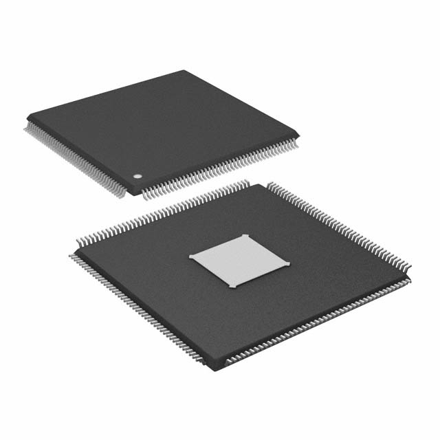
- Part No.:
- TC265D40F200WBBLXUMA1
- Manufacturer:
- Infineon Technologies
- Category:
- Microcontrollers
- Package:
- 176-LQFP Exposed Pad
- Datasheet:
-
 TC265D40F200WBBLXUMA1.pdf
- Description:
- IC MCU 32BIT 2.5MB FLASH 176LQFP
- Quantity:
- Payment:

- Shipping:

Inventory:1,107
Please send an inquiry. Send us your inquiry, and we will respond immediately.
Product details
Overview
TC265D40F200WBBLXUMA1 from Infineon Technologies is a 32-bit automotive microcontroller based on the TriCore™ v1.6.1 architecture, featuring 2 MB embedded Flash, 256 KB SRAM, and integrated CAN FD, LIN, and SENT interfaces. It operates across -40°C to 150°C ambient temperature, supports ASIL-D functional safety per ISO 26262, and targets engine control units (ECUs) requiring real-time deterministic processing.
For engineers reviewing the TC265D40F200WBBLXUMA1 datasheet, TC265D40F200WBBLXUMA1 pinout, TC265D40F200WBBLXUMA1 application, or TC265D40F200WBBLXUMA1 equivalent, key selection criteria include its dual-core lockstep configuration, 200 MHz CPU clock, hardware safety module (HSM), Flash ECC protection, and qualification per AEC-Q100 Grade 0.
Technical Context
This MCU integrates a TriCore™ CPU core with a separate Safety Core for runtime monitoring, enabling ASIL-D compliance in safety-critical powertrain applications. It includes a Peripheral Server Unit (PSU) for configurable I/O routing, a Multi-Channel DMA controller supporting up to 128 channels, and a System Memory Management Unit (SMMU) for memory access arbitration and protection.
The device implements a scalable peripheral set including six GPT12 timers, four ASC interfaces with baud rate generation up to 3 Mbit/s, two DSADC modules with 12-bit resolution and 1.5 MSPS sampling rate, and a 12-bit SAR ADC with 48 channels and programmable scan sequencing.
Key Specifications
| Parameter | Value and Actual Design Meaning |
|---|---|
| CPU Core | TriCore™ v1.6.1 dual-core (main + safety lockstep), 200 MHz max frequency |
| Memory | 2 MB on-chip Flash with ECC, 256 KB SRAM with parity, 64 KB instruction TCM |
| Temperature Range | -40°C to +150°C ambient, qualified per AEC-Q100 Grade 0 |
| Safety Certification | ISO 26262 ASIL-D compliant with integrated Hardware Safety Module (HSM) |
| Communication Interfaces | 6× CAN FD (up to 5 Mbit/s), 4× LIN, 2× SENT, 2× SPI, 2× I²C |
| Analog Peripherals | 12-bit SAR ADC (48 ch, 1.2 MSPS), 2× DSADC (12-bit, 1.5 MSPS, 4 ch each) |
Pinout & Package
Package: PG-LQFP-144-27 (144-pin Low-Profile Quad Flat Package, 20 mm × 20 mm, 0.5 mm pitch, exposed thermal pad).
| Pin/Terminal | Circuit Role | Design Meaning |
|---|---|---|
| VDDP | Core Power Supply | 1.3 V ±3% supply for CPU and logic; requires low-noise decoupling |
| VDDA | Analog Power Supply | 5 V ±5% supply for ADC/DSADC; isolated analog domain reference |
| OSC_IN / OSC_OUT | Crystal Oscillator Interface | Supports 1–40 MHz external crystal; feeds PLL for system clock generation |
| TRSTN | JTAG Debug Reset | Active-low asynchronous reset input for boundary-scan and debug initialization |
| ETH_RXD0 / ETH_TXD0 | Ethernet PHY Interface | 100BASE-TX differential pair; requires 50 Ω impedance matching and magnetics |
Key Features
| Feature | Design Value |
|---|---|
| Dual-core lockstep execution | Enables real-time fault detection with zero-latency comparison between main and safety core outputs |
| Hardware Safety Module (HSM) | Independent RISC-based safety core with dedicated RAM/ROM, supports ASIL-D runtime checks and safe boot |
| Flash ECC with error injection test mode | Single-bit correction and double-bit detection with built-in diagnostic test capability per ISO 26262 |
| Configurable Peripheral Server Unit (PSU) | Runtime-reconfigurable I/O mapping allows dynamic pin function assignment without firmware restart |
| Multi-channel DMA with scatter-gather support | Offloads CPU from data movement; enables zero-copy transfers between peripherals and memory regions |
Applications
| Engine Control Unit (ECU) | Transmission Control Module (TCM) |
|---|---|
Use Scenario: Real-time combustion timing, fuel injection pulse width, and knock detection in gasoline direct injection engines. IC Role / Device Role / Timing Role: Primary control MCU executing ASIL-D safety-critical functions with dual-core lockstep and HSM supervision. Use Value: Meets <10 µs worst-case interrupt latency and supports deterministic 10 kHz control loop execution with hardware-accelerated math units. | Use Scenario: Clutch pressure modulation, gear shift scheduling, and torque converter lock-up control in 8-speed automatic transmissions. IC Role / Device Role / Timing Role: Central timing and actuator driver MCU with synchronized PWM outputs and SENT feedback decoding. Use Value: Delivers 20 ns PWM edge resolution and supports 12 independent SENT receivers for real-time sensor fusion. |
| Electric Power Steering (EPS) | Battery Management System (BMS) Controller |
Use Scenario: Motor current control, road torque estimation, and assist torque blending using multi-sensor inputs (torque, angle, speed). IC Role / Device Role / Timing Role: Safety-critical motor control MCU with integrated DSADC for high-speed current sensing and GPT12 for precise PWM generation. Use Value: Achieves 1.5 MSPS current sampling with hardware-triggered ADC conversion and zero-latency dead-time insertion in gate drivers. | Use Scenario: Cell voltage monitoring, thermal management, state-of-charge estimation, and isolation barrier communication in high-voltage traction batteries. IC Role / Device Role / Timing Role: Master BMS controller interfacing with isolated analog front-ends and daisy-chained digital sensors via SPI/CAN FD. Use Value: Supports simultaneous 48-cell voltage measurement with <1 mV accuracy and 12-bit SAR ADC scan sequencing triggered by hardware timer events. |
Equivalent & Alternatives
The following parts are listed as comparable options for similar automotive microcontroller applications.
| Alternative Part | Technical Difference | Application Difference | Selection Advice |
|---|---|---|---|
| TC275T64F200WCKXUMA1 | Higher Flash (4 MB), larger package (PG-LQFP-176), no Ethernet MAC | Targeted at complex chassis control where extended code space outweighs Ethernet need | Select when >2 MB Flash required and Ethernet interface is not needed |
| TC375L64F200NACKXUMA1 | TriCore™ v2.0 core, 300 MHz, 4 MB Flash, 512 KB SRAM, no DSADC | Designed for next-gen ADAS domain controllers requiring higher compute throughput | Select for new designs needing >200 MHz performance and future-proof architecture |
Compared with TC275T64F200WCKXUMA1 and TC375L64F200NACKXUMA1, the TC265D40F200WBBLXUMA1 offers optimal balance of ASIL-D safety features, Ethernet connectivity, and thermal robustness for powertrain ECUs operating at 150°C, without over-provisioning Flash or CPU resources.
Availability
TC265D40F200WBBLXUMA1 is available at Aetrix Electronics and suitable for engine control units, transmission control modules, and electric power steering systems requiring stable component supply under extended temperature and automotive qualification requirements.
Supply support for TC265D40F200WBBLXUMA1 includes scheduled delivery planning, volume procurement assistance, BOM continuity management, traceable sourcing, and lifecycle availability coordination for OEM customers, industrial embedded developers, connected-device designers, and electronics production programs.
Manufacturer
Infineon Technologies is a German semiconductor manufacturer specializing in power semiconductors, automotive MCUs, and security solutions, with global manufacturing and R&D centers.
The AURIX™ TC2xx family delivers scalable, safety-certified microcontrollers for automotive powertrain, chassis, and body applications, emphasizing real-time determinism, functional safety, and thermal resilience.
FAQ
What is the maximum junction temperature rating for TC265D40F200WBBLXUMA1?
The device is rated for a maximum junction temperature of +175°C, validated under AEC-Q100 Grade 0 conditions (−40°C to +150°C ambient). Thermal derating curves and PCB layout guidelines for thermal pad soldering are provided in the hardware design manual, and the exposed pad must be connected to a minimum 4-layer thermal plane for sustained operation at 150°C ambient.
Does TC265D40F200WBBLXUMA1 support secure boot and cryptographic acceleration?
Yes - it includes a dedicated Hardware Security Module (HSM) with AES-128/256, SHA-256, RSA-2048, and TRNG support, plus secure boot ROM that validates signed firmware images before execution. The HSM operates independently of the main TriCore™ core and provides tamper-resistant key storage with physical unclonable function (PUF)-derived keys.
Can TC265D40F200WBBLXUMA1 operate without an external crystal oscillator?
No - the device requires an external crystal (1–40 MHz) on OSC_IN/OSC_OUT pins to generate the base clock for its PLL. Internal RC oscillators are only for fail-safe startup and cannot meet timing accuracy or stability requirements for ASIL-D operation; they are disabled after successful crystal lock detection during boot.
How many CAN FD interfaces does TC265D40F200WBBLXUMA1 support, and what is their data rate capability?
It integrates six CAN FD controllers with transceiver-independent physical layer support, each capable of up to 5 Mbit/s data phase speed and 1 Mbit/s arbitration phase. All six channels support ISO 11898-1:2015 compliance, flexible data-length up to 64 bytes, and hardware message filtering with 128 configurable ID filters per channel.
TC265D40F200WBBLXUMA1 Specifications
- Product attributes
- Attribute value
- Manufacturer:
- Infineon Technologies
- Package/Case:
- 176-LQFP Exposed Pad
- Series:
- AURIX™
- Packaging:
- Tape & Reel (TR)
- Product Status:
- Active
- Programmable:
- Not Verified
- Core Processor:
- TriCore™
- Core Size:
- 32-Bit Dual-Core
- Speed:
- 200MHz
- Connectivity:
- ASC, CANbus, Ethernet, FlexRay, HSSL, I2C, LINbus, MSC, PSI5, QSPI, SENT
- Peripherals:
- DMA, WDT
- Number of I/O:
- 112
- Program Memory Size:
- 2.5MB (2.5M x 8)
- Program Memory Type:
- FLASH
- EEPROM Size:
- 96K x 8
- RAM Size:
- 240K x 8
- Voltage - Supply (Vcc/Vdd):
- 1.17V ~ 5.5V
- Data Converters:
- A/D 50x12b SAR, Sigma-Delta
- Oscillator Type:
- External
- Operating Temperature:
- -40°C ~ 150°C (TA)
- Grade:
- -
- Qualification:
- -
- Mounting Type:
- Surface Mount
- Supplier Device Package:
TC265D40F200WBBLXUMA1 FAQ
1.How can I place an order for TC265D40F200WBBLXUMA1 through Aetrix?
Please submit a Request for Quotation (RFQ) for TC265D40F200WBBLXUMA1 on Aetrix. Our sales agent will provide a competitive quotation and guide you through the order confirmation once you accept the terms.
2.Are the price and stock information for TC265D40F200WBBLXUMA1 reliable?
The price and inventory of TC265D40F200WBBLXUMA1 are updated periodically and may fluctuate due to market conditions. Stock and pricing data are typically refreshed every 24 hours. Quotation validity for TC265D40F200WBBLXUMA1 is usually 5 days.
3.What payment methods are accepted for TC265D40F200WBBLXUMA1?
We accept Wire Transfer, PayPal, Credit Card, Western Union, MoneyGram, and Escrow for TC265D40F200WBBLXUMA1 transactions.
Note: Certain payment methods may incur a processing fee.
4.How is shipping managed for TC265D40F200WBBLXUMA1?
TC265D40F200WBBLXUMA1 orders can be shipped via leading logistics carriers, including DHL, UPS, FedEx, TNT, or Registered Mail.
Once your TC265D40F200WBBLXUMA1 order is processed, you will receive an email with the shipment details and tracking number.
Note: Tracking information may take up to 24 hours to appear. Express delivery typically takes 3–5 business days.
5.How can I obtain technical support or documentation for TC265D40F200WBBLXUMA1?
For technical support, including TC265D40F200WBBLXUMA1 datasheets, pinout diagrams, or application guidance, please contact our engineering support team. They can provide detailed documentation and assistance for your TC265D40F200WBBLXUMA1 requirements.
6.How does Aetrix verify that TC265D40F200WBBLXUMA1 is sourced from the original manufacturer or authorized distributors?
All TC265D40F200WBBLXUMA1 products on Aetrix are procured from qualified distributors and authorized channels. Our dedicated quality assurance team conducts strict verification, including traceability checks and, if necessary, third-party testing. This ensures that TC265D40F200WBBLXUMA1 meets industry standards.
7.What is the process for return or replacement of TC265D40F200WBBLXUMA1?
All TC265D40F200WBBLXUMA1 units undergo pre-shipment inspection (PSI). If there is an issue with TC265D40F200WBBLXUMA1, returns or replacements are accepted under the following conditions:
1.Quantity discrepancies, incorrect items, or visible external defects (such as breakage or corrosion), acknowledged by Aetrix.
2.The issue is reported within 90 days of delivery.
3.The TC265D40F200WBBLXUMA1 part is unused and in its original packaging.
Return procedure for TC265D40F200WBBLXUMA1:
1.Submit a request within 90 days.
2.Obtain a Return Material Authorization (RMA) from Aetrix.
TC265D40F200WBBLXUMA1 Tags

-
ATTINY4-TSHR
Microchip Technology
-
ATTINY10-TSHR
Microchip Technology
-
ATTINY10-TS8R
Microchip Technology

-
ATTINY202-SSNR
Microchip Technology
-
ATTINY202-SSFR
Microchip Technology
-
ATTINY402-SSNR
Microchip Technology

-
PIC16F15213T-I/MF
Microchip Technology
-
PIC16F15213-E/MF
Microchip Technology

-
PIC10F200T-I/OT
Microchip Technology
-
ATTINY412-SSNR
Microchip Technology
-
PIC10F202T-I/OT
Microchip Technology

-
ATTINY404-SSNR
Microchip Technology
Tech Hub

Comparator circuit design covering voltage thresholds, input limits, open-collector outputs, LM393 wiring, op-amp differences, hysteresis, timing, window detection and practical fault diagnosis.

Schmitt triggers use separate rising and falling thresholds to stabilize slow or noisy signals. This guide covers hysteresis, 74HC14 and 74HCT14 selection, comparator calculations, RC oscillators and p…

Counterfeit components can hide behind convincing markings and passing basic function tests. This engineering reference covers source traceability, external inspection, X-ray, XRF, electrical testing, …

A practical engineering and sourcing framework covering lifecycle verification, lifetime-buy calculations, replacement qualification, supplier checks and counterfeit-risk controls.

TTL and CMOS logic families differ in thresholds, loading, output drive, power and timing. This engineering guide compares 74HC and 74HCT, calculates noise margins and checks 3.3 V/5 V compatibility.

A practical engineering guide to 3.3V and 5V logic compatibility, input thresholds, resistor dividers, translator ICs, MOSFET level shifting, I2C pull-ups, timing limits and power-sequencing risks.

The 74HC595 uses push-pull logic outputs, while the TPIC6B595 uses 50 V open-drain DMOS sinks for higher-power loads. This guide compares timing, current limits, 3.3 V interfacing, load wiring, thermal…

The 74HC595 converts serial data into eight stable parallel outputs. This guide covers pin functions, shift and storage timing, OE and MR behavior, drive-current limits, cascading, voltage compatibilit…

A technical comparison of level-sensitive latches and edge-triggered flip-flops, covering timing windows, setup and hold limits, master–slave operation, time borrowing, race-through, HDL inference and…

A D latch stores one bit while Enable controls when data can pass. This reference covers gate-level operation, truth tables, transparency, setup and hold timing, LE versus OE, common ICs and practical …


